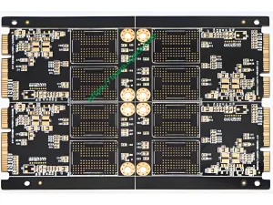
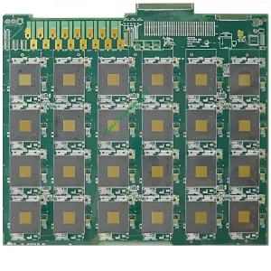
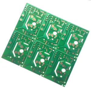
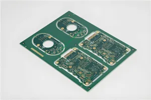
Introduction to the 18Layers Communication Base Station PCB
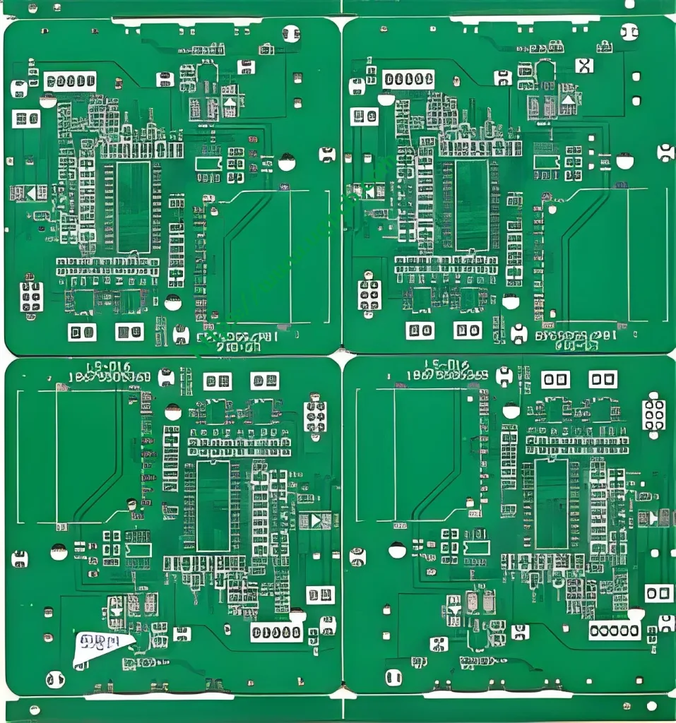
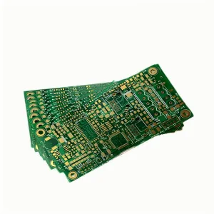
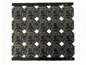
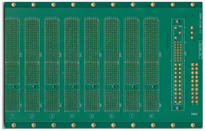
The 18Layers Communication Base Station PCB is a sophisticated and high-performance printed circuit board designed specifically for use in communication base stations. This PCB offers exceptional durability, مصداقية, and efficiency, making it an ideal choice for critical communication infrastructure applications.
Key Features and Specifications
مادة
- مادة: The PCB is made from Panasonic M6, a high-quality material known for its excellent electrical properties and thermal stability. This ensures that the PCB can withstand harsh environmental conditions and maintain optimal performance.
Layers and Copper Thickness
- طبقات: With 18 طبقات, this PCB provides extensive space for complex circuit designs required in advanced communication systems.
- سمك النحاس: The copper thickness ranges from 0.5 ل 1 أوقية, allowing for robust signal transmission and power distribution across the board.
Dimensions and Surface Treatment
- سمك الانتهاء: The PCB has a finished thickness of 2.0mm, which provides structural integrity and mechanical strength.
- المعالجة السطحية: It features an immersion gold surface treatment. This not only enhances the aesthetic appeal but also improves solderability, corrosion resistance, and contact reliability.
Precision Design
- Trace/Space: Featuring precise trace/space measurements of 4mil/4mil (0.1MM/0.1MM), this PCB ensures high-density interconnectivity with minimal crosstalk and signal loss.
- Min Hole: The minimum hole size is 0.2mm (8ميل), enabling fine-pitch components and high-density layouts.
Special Processes
- Special Process: The PCB incorporates a metal edging process, which adds extra strength and protection to the edges, enhancing the overall durability and lifespan of the board.
Applications
The 18Layers Communication Base Station PCB is primarily used in communication base station applications where high reliability and performance are crucial. وتشمل هذه:
- Mobile network base stations
- Radio frequency (RF) transceivers
- Microwave communication systems
- Data center networking devices
Production Process
The manufacturing process of the 18Layers Communication Base Station PCB involves several meticulous steps to ensure the highest quality standards:
- Material Selection: High-grade Panasonic M6 material is selected for its superior electrical properties and durability.
- Layer Stacking: ال 18 layers are carefully stacked and bonded together using advanced laminating techniques.
- Etching and Drilling: Precision etching and drilling processes create the intricate circuit patterns and holes necessary for component placement.
- Plating and Soldermask Application: Immersion gold plating and soldermask application provide the final surface treatment, ensuring excellent conductivity and protection against environmental factors.
- ضبط الجودة: Each PCB undergoes rigorous testing and inspection to meet strict quality criteria before being packaged for shipment.
خاتمة
The 18Layers Communication Base Station PCB is a highly specialized product designed to meet the demanding requirements of modern communication infrastructure. Its advanced materials, precision design, and stringent manufacturing processes make it a reliable choice for any high-performance communication system. Whether you are building mobile network base stations or data center equipment, this PCB offers unmatched reliability and performance.
 شعار UGPCB

