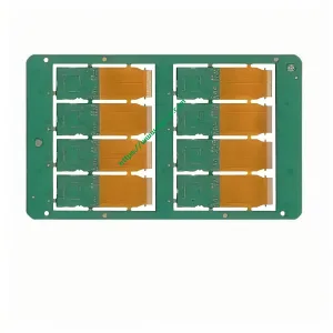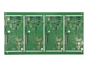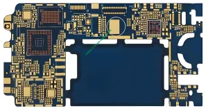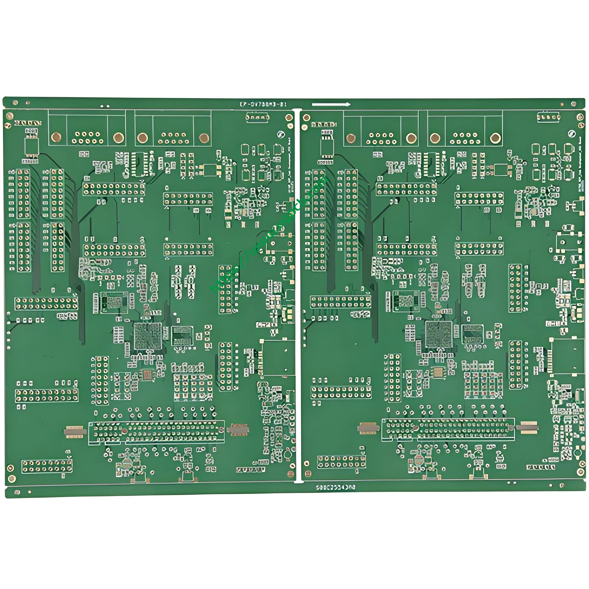
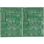
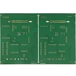
Definition of HDI PCB
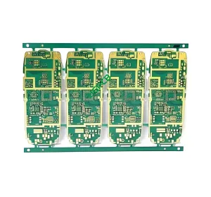
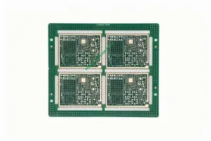
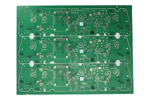
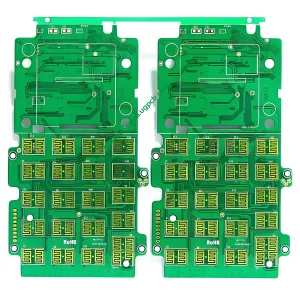
ربط الكثافة العالية (مؤشر التنمية البشرية) is simply a PCB with a higher number of interconnects in the smallest footprint. This leads to miniaturization of the circuit board. Components are placed closer together and board space is significantly reduced, but functionality is not compromised.
Characteristics of HDI PCB
More precisely, a PCB with an average of 120 ل 160 pins per square inch is considered an HDI PCB. HDI designs combine dense component placement and versatile routing. HDI popularized microporous technology, creating denser circuits by implementing microvias, فيا مدفونة, and blind vias. Reduced drilling of copper is a feature of HDI designs.
Advantages of HDI PCB
Extraordinary Versatility
HDI boards are ideal when weight, فضاء, مصداقية, and performance are the main concerns.
تصميم مدمج
The combination of blind, مدفون, and micro vias reduces board space requirements.
Better Signal Integrity
HDI utilizes via-in-pad and blind via technology. This helps keep components close to each other, reducing signal path lengths. HDI technology removes through-hole stubs, thus reducing signal reflections, thereby improving signal quality. لذلك, it significantly improves signal integrity due to shorter signal paths.
موثوقية عالية
The implementation of stacked vias makes these boards a super barrier against extreme environmental conditions.
فعالة من حيث التكلفة
The functionality of a standard 8-layer through-hole board (ثنائي الفينيل متعدد الكلور القياسي) can be reduced to a 6-layer HDI board without compromising the quality. This makes HDI PCBs a cost-effective solution.