و,ثنائي الفينيل متعدد الكلور, تخصيص PCBA وPECVD, النماذج الأولية والتصنيع المنتج

تحميل | عن | اتصال | خريطة الموقع

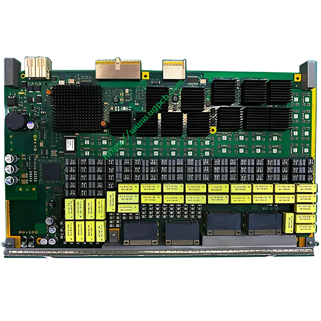
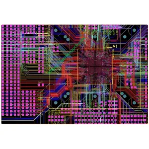
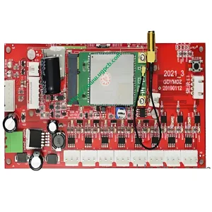
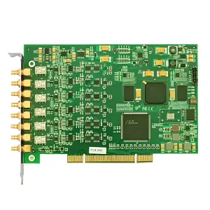
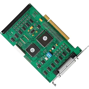
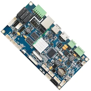
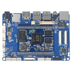
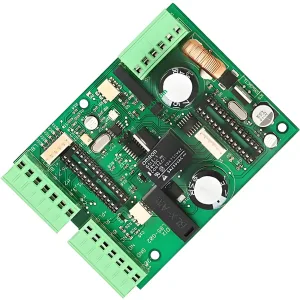
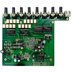
WiFi PCBA control equipment copy board

اسم: WiFi PCBA control equipment copy board

The number of layers that can be copied: 1-32 طبقات

الحد الأدنى لعرض الخط وتباعد الأسطر: 3ميل

الحد الأدنى لفتحة الليزر: 4ميل

الحد الأدنى من الفتحة الميكانيكية: 8ميل

سمك رقائق النحاس: 18-175سم (معيار: 18سم35سم70سم)

قوة قشر: 1.25ن / مم

الحد الأدنى لقطر ثقب التثقيب: جانب واحد: 0.9ملم/35 مل

الحد الأدنى لقطر الثقب: 0.25ملم/10 مل

التسامح الفتحة: .8φ0.8mm ± 0.05mm

Hole tolerance: ±0.05mm

Hole wall copper thickness: double-sided/multi-layer: ≥2um/0.8mil

Hole resistance: double-sided/multi-layer: ≤300цΩ

الحد الأدنى لعرض الخط: 0.127mm/5mil

Minimum pitch: 0.127mm/5mil

المعالجة السطحية: rosin spray tin electric gold, anti-oxidation, chemical gold, carbon oil

Warpage: ≤0.7%

  • تفاصيل المنتج

Overview of UGPCB’s Services

UGPCB provides a one-stop solution from WiFi PCB manufacturing to WiFi module assembly services.

WiFi Module Prototype PCB Assembly Services

Frequency Options

All WiFi module prototype PCB assembly services are available in either a 2.4 GHz or 5 GHz version.

Antenna Support

These services support both chip antennas and external antennas.

Integration with Customer Carrier Boards

Using our schematics as reference designs, module designs can be integrated into customer carrier board designs.

السابق:

التالي:

ترك الرد

ترك رسالة