
Mastering PCB Impedance Control: Advanced Strategies for High-Speed Circuit Design
Figure 1: Critical impedance-controlled traces in multilayer PCB design
The Critical Role of Impedance Control in Modern Electronics
Why Impedance Matching Matters in High-Frequency Designs
In high-speed digital systems operating above 1 GHz, ثنائي الفينيل متعدد الكلور traces transform from simple conductors to complex transmission lines where characteristic impedance (Z₀) becomes paramount. When Z₀ mismatches occur between components, signal reflections can reach 35% of incident power, causing waveform distortion and timing errors that cripple system performance.
Key consequences of poor impedance control:
- Signal integrity degradation: Rise time degradation up to 40% in DDR4 interfaces
- EMI radiation spikes: Mismatched lines can increase radiated emissions by 15-20dB
- Power integrity issues: Return path discontinuities create ground bounce
Fundamental Impedance Concepts
Characteristic Impedance Formula for Microstrip:
Z₀ = \frac{87}{\sqrt{ε_r + 1.41}} \ln\left(\frac{5.98H}{0.8W + ت}\right)
Where:
- ε_r = Dielectric constant (FR4: 4.2-4.7, Rogers 4350B: 3.48)
- H = Dielectric thickness (مم)
- W = Trace width (مم)
- T = Copper thickness (أوقية)
Differential Pair Calculation:
Z_{diff} = 2Z₀ \left(1 - 0.48e^{-0.96S/H}\right)
S = Pair spacing, H = Dielectric height
Five Pillars of PCB Impedance Engineering
1. Material Selection Matrix
| Material Type | ε_r @10GHz | Loss Tangent | Cost Index |
|---|---|---|---|
| فر-4 | 4.5 | 0.02 | $ |
| Rogers 4350B | 3.48 | 0.0037 | $$$ |
| Isola I-Tera | 3.45 | 0.0031 | $$$$ |
| PTFE Composite | 2.2-3.0 | 0.0009 | $$$$$ |
Table 1: High-frequency laminate comparison
2. Stackup Architecture Principles
Optimal 12-Layer HDI Stackup for 25Gbps Signals:
- L1: Signal (0.5أوقية)
- L2: Ground
- L3: Signal (3.5mil dielectric)
- L4: قوة
- L5: Signal (High-speed)
- L6: Ground
… Mirror symmetric structure
Critical parameters:
- Dielectric thickness tolerance: ±10% maximum
- Copper roughness: <2μm RMS for >10GHz
- Sequential lamination for impedance continuity
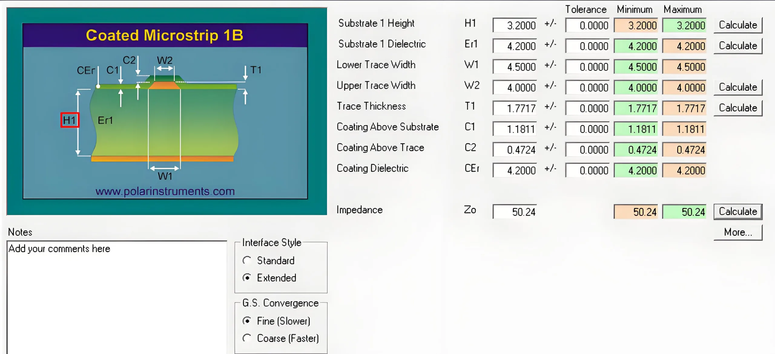
3. Advanced Calculation Methodologies
Three-Step Impedance Validation Process:
- Initial Estimation:
Use empirical formula:W ≈ \frac{100H}{\sqrt{ε_r}} \quad (\text{50Ω microstrip})
- Precision Simulation:
- Polar SI9000 for multi-layer structures
- Rogers MWI-2017 for RF/microwave lines
- Post-production Verification:
TDR measurements with <5% tolerance
 Figure 2: PCB impedance engineering workflow
4. Manufacturing Process Controls
Critical Tolerance Factors:
| Parameter | Typical Tolerance | Impact on Z₀ |
|---|---|---|
| Etching width | ±0.5mil | ±3Ω |
| Dielectric thickness | ±10% | ±8Ω |
| Copper weight | ±0.2oz | ±2Ω |
| Soldermask | 0.3-0.5ميل | ±1.5Ω |
Data from IPC-2141A standards
Mitigation Strategies:
- Use compensated artwork (0.75× etch factor)
- Implement automated optical inspection (الهيئة العربية للتصنيع)
- Specify controlled impedance test coupons
5. Cutting-Edge Tools Ecosystem
Industry-Leading Software Solutions:
- Polar Instruments Si9000e
- 2D field solver with 47 transmission line models
- Batch processing for complex designs
- Rogers MWI-2017
- Specialized for microwave designs up to 110GHz
- Integrated material database with 50+ substrates
- Cadence Sigrity Aurora
- 3D EM simulation with <2% error margin
- DDR5/PCIe6.0 compliance checking
- Altium Impedance Profiler
- Real-time impedance visualization
- Automated stackup validation
Practical Design Guidelines for Engineers
Golden Rules for First-Time-Right Designs
- 3W Rule for Crosstalk Control:
S ≥ 3×W \quad (\text{Where S = trace spacing})
- Length Matching Priorities:
- Differential pairs: <5mil intra-pair mismatch
- Bus signals: <100ps delay skew
- Via Optimization Techniques:
- Use 8-12mil diameter for 10Gbps signals
- Backdrilling for stub length <15% of rise time
- Termination Strategies:
Type طلب Power Cost Series 22Ω Source-end Low Parallel 50Ω End-point عالي AC Capacitive DDR Memory Interfaces Medium
Future Trends in Impedance Management
Emerging Technologies Impact
- 5G mmWave Challenges:
- 28/39GHz bands require ±1Ω tolerance
- Laser ablation for 2μm line width control
- Advanced Packaging Integration:
- 3D IC with TSV impedance matching
- Hybrid substrate PCB-Flex designs
- AI-Driven Impedance Optimization:
- Neural networks predicting manufacturing variations
- Generative design for multi-constraint solutions
Take action to get a quote
UGPCB holds a leading position in both the PCB (لوحة الدوائر المطبوعة) and PCBA (Printed Circuit Board Assembly) sectors, making it an industry leader. UGPCB boasts a highly experienced PCB design team that excels in PCB impedance control, ranking at the forefront of the industry. If you have any questions or design requirements related to PCB impedance, please contact our professional technical staff for technical support or to take action and request a competitive quote today.
