
Hybridplatine
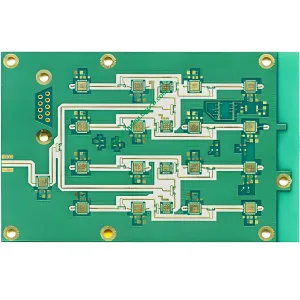
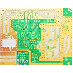
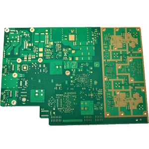
UGPCB Hybrid PCB Solutions: Unlocking Cross-Material Integration for High-Frequency and High-Density Design
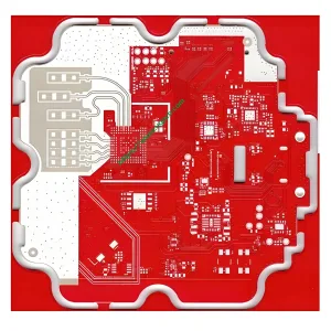
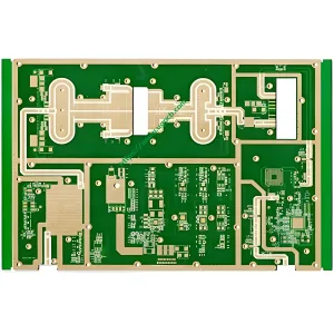
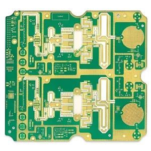
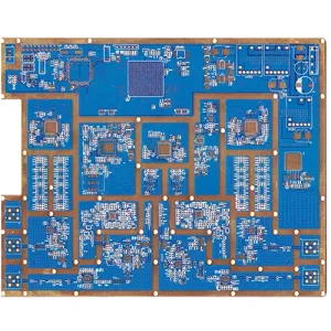
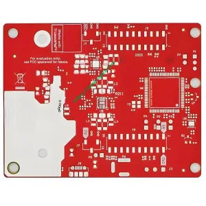
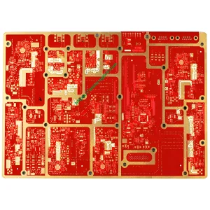
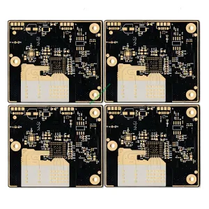
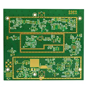
As a leading global provider of hybrid PCB (Hyrid PCB) technology solutions, UGPCB specializes in high-frequency, high reliability, and complex system integration. Our focus is on resolving the performance and cost contradictions inherent in traditional single-material PCBs. By utilizing multi-material lamination processes (such as combining FR-4 with Rogers/PTFE) and heterogeneous interconnect architectures, our hybrid PCB technology offers a balanced solution for signal integrity, thermal management, and cost control across demanding applications like 5G communications, Automobilelektronik, und Luft- und Raumfahrt.
Core Advantages: Professional Barriers in Cross-Material Collaborative Design
Material Compatibility Innovation
- High-Frequency Cost-Optimized Stacking: By laminating Rogers RO4000®/Taconic RF-35 with FR-4, we achieve a 30% reduction in high-frequency area costs while ensuring Dk±0.05 stability at 10GHz.
- CTE Dynamic Matching Technology: Combining low CTE core materials (z.B., Isola I-Tera® MT) with flexible PCB substrates (DuPont Pyralux®), we mitigate thermal cycle delamination risks and pass IPC-6012 6A level thermal shock tests (-55℃↔150℃, 1,000 Zyklen).
Signal and Power Integrity Assurance
- Cross-Region Impedance Control: Using Ansys HFSS full-wave simulation, we ensure seamless transition between high-frequency areas (50Ω±2%) and power areas (1mΩ current flow), reducing resonance risks.
- 3D Shielding Architecture: Embedded metallized via walls (Isolierung >60dB@10GHz) and localized ground plane segmentation techniques meet stringent EMC standards such as CISPR 25/ISO 11452-2.
High-Density Hybrid PCB Manufacturing Process
- Precision Interlayer Alignment: Laser direct imaging (LDI) ensures layer-to-layer misalignment <±25μm, supporting 0.1mm microvias and over 20 layers of mixed stacking.
- Vacuum Lamination Process: Segmented pressure control eliminates bubbles at the FR-4/PTFE interface, achieving ±3% dielectric thickness uniformity.
Typical Application Scenarios and Technical Benchmarks
- 5G Basisstation AAU: 32-layer hybrid PCB (Rogers RO4835™+FR-4) achieves insertion loss ≤0.25dB/inch at n258 band and VSWR<1.3, aiding Massive MIMO antenna mass production.
- Automotive Intelligent Driving: 12-layer hybrid board (MEGTRON®6+high Tg FR-4) integrates 77GHz millimeter wave radar and in-vehicle Ethernet, passing AEC-Q200 Grade 2 Zertifizierung.
- Satellite Communication Terminal: Aluminum-based hybrid PCB (metal core+PTFE) supports Ka-band phased array antenna EIRP>55DBM, meeting IPC-6012DS aerospace reliability standards.
Comprehensive PCB Services and Certification System
- Design Verification: Offers Cadence Allegro-based hybrid stack simulation, Flotherm® thermal distribution analysis, and HALT accelerated life testing (20G vibration/85℃/85%RH).
- Rapid Delivery: 8-layer hybrid PCB prototype delivery within 72 Std., supporting ODB++/IPC-2581 format collaborative review.
- Industry Certifications: ISO 9001/IATF 16949 system certifications, NADCAP military qualifications, 100% compliance with IPC-6013/6018 hybrid PCB standards.
Why Choose UGPCB Hybrid PCB?
- 15 Years of Technological Accumulation: A database of over 200 successful high-frequency hybrid PCB cases covering millimeter wave/terahertz frontier fields.
- Cost-Controlled Innovation: Patented material combination solutions reduce customer BOM costs by 15%-40%.
- Zero-Risk Mass Production: DFM/DFA full cycle involvement ensures stable mass production yield >99.5%.
Get Your Custom Solution Now!
Visit the UGPCB Hybrid PCB section page to submit your requirements and receive a free stack simulation report!
 UGPCB-LOGO

WeChat
Scannen Sie den QR-Code mit WeChat