
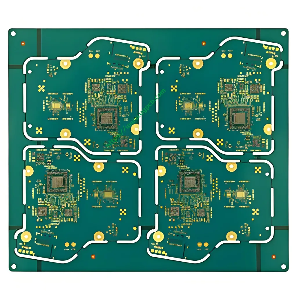
Technical Features and Applications of HDI PCBs
Impedance Specifications
- 50 Ω Antenna
- 90Oh & 100Ω Differential Impedance
Anwendungen
Unterhaltungselektronik
- Cell Phones
- Tabletten
- Ultrabooks
- E-Readers
- MP3 Players
- GPS
- Portable Game Consoles
- DSCs (Digital Still Cameras)
- Cameras
- LCD TVs
- POS Terminals
Hochdichte Interconnect (HDI) PCB Usage
Mobile and Portable Devices
HDI PCBs are widely used to reduce the weight and overall size of products, as well as improve the electrical performance of devices. High-density PCBs are often found in:
- Mobile Phones
- Touch Screen Devices
- Laptops
- Digital Cameras
- 4G Network Communications
Other Applications
HDI PCB technology also plays an important role in:
- Medizinische Ausrüstung
- Electronic Aircraft Components
The Future of HDI PCB Technology
The possibilities for high-density interconnect PCB technology seem almost limitless.


