
Overview of the 18Layers 3oz Copper Power PCB
The 18Layers 3oz Copper Power PCB is a high-density, multilayer power board designed for applications requiring robust electrical performance and reliability. Diese PCB ist ideal für komplexe elektronische Systeme, die hohe Leistung und Signalintegrität verwalten müssen.
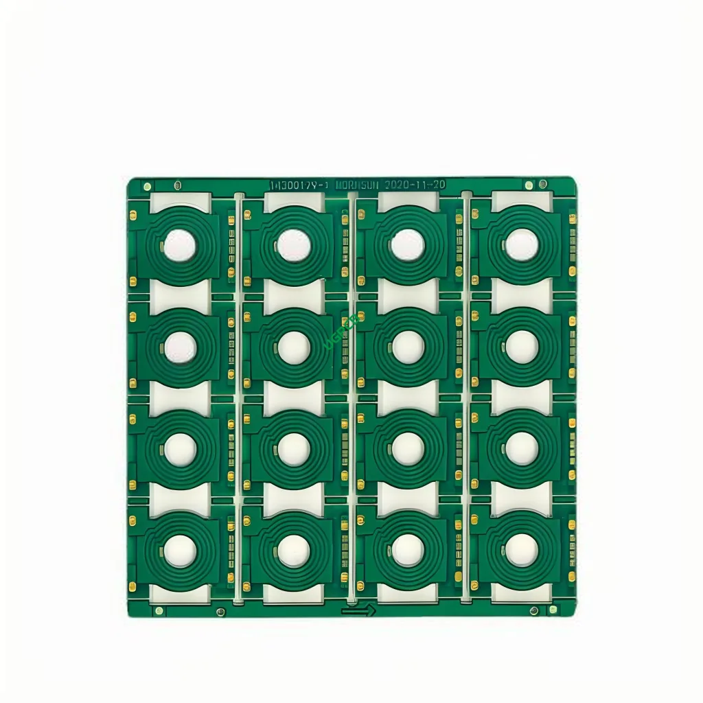
What is an 18Layers 3oz Copper Power PCB?
An 18Layers 3oz Copper Power PCB is a printed circuit board (Leiterplatte) mit 18 layers of copper traces, each weighing 3 Unzen pro Quadratfuß. This type of PCB is specifically designed for power applications, where it needs to handle large currents and provide stable electrical connections.
Entwurfsanforderungen
The design requirements for an 18Layers 3oz Copper Power PCB are stringent to ensure its performance and reliability:
- Material: EM827, Ausgewählt für seine hervorragenden elektrischen und thermischen Eigenschaften.
- Schichtzahl: 18 Schichten für komplexe und dichte Schaltungsdesigns aufnehmen.
- Farbe: Grün/Weiß für einfache Identifizierung und ästhetische Anziehungskraft.
- Fertige Dicke: 4.0MM zur Bereitstellung struktureller Integrität und Haltbarkeit.
- Kupferdicke: 3OZ, um eine angemessene Leitfähigkeit und Wärmeableitung zu gewährleisten.
- Oberflächenbehandlung: Eintauchen Gold, um die Lötlichkeit und Korrosionsresistenz zu verbessern.
- Copper Thickness in Hole: 70UM for better electrical connectivity.
- Line Width: 0.3mm to support fine circuit patterns.
- Minimum Aperture: 0.4mm to allow precise component placement.
Wie funktioniert es?
The 18Layers 3oz Copper Power PCB works by providing a platform for various electronic components to be interconnected through conductive pathways. Diese Wege, oder Spuren, sind aus Kupfer und sind auf die Brett geätzt. The immersion gold surface treatment ensures that these traces remain conductive and resistant to environmental factors.
Anwendungen
The primary application of the 18Layers 3oz Copper Power PCB is in power electronics where it manages and regulates the flow of electrical power. Dies schließt:
- Power supplies
- Motor drives
- Renewable energy systems
- Industrial Control Systems
Einstufung
Basierend auf seinen Funktionen und Anwendungen, the 18Layers 3oz Copper Power PCB can be classified as a high-power PCB designed for demanding power applications. This classification highlights its capability to handle large currents and provide stable electrical connections.
Materialzusammensetzung
The core material used in the 18Layers 3oz Copper Power PCB is EM827, a high-performance laminate material known for its excellent mechanical, Thermal-, und elektrische Eigenschaften. This material ensures that the PCB can withstand the demands of power applications.
Leistungseigenschaften
The performance characteristics of the 18Layers 3oz Copper Power PCB include:
- High power handling capacity
- Hervorragende Signalintegrität
- Vorgesetzter thermisches Management
- Robuste mechanische Stärke
- Langfristige Stabilität
Strukturelle Details
The structural details of the 18Layers 3oz Copper Power PCB are as follows:
- Schichtzahl: 18 Schichten
- Fertige Dicke: 4.0mm
- Kupferdicke: 3OZ
- Oberflächenbehandlung: Immersionsgold
- Copper Thickness in Hole: 70UM
- Line Width: 0.3mm
- Minimum Aperture: 0.4mm
Funktionen und Vorteile
The key features and benefits of the 18Layers 3oz Copper Power PCB include:
- Interkonnektivität mit hoher Dichte
- Excellent power handling capacity
- Robuste mechanische Konstruktion
- Zuverlässige langfristige Leistung
- Ästhetische Farboptionen (Grün/Weiß)
Produktionsprozess
The production process of the 18Layers 3oz Copper Power PCB involves several steps, einschließlich:
- Materialauswahl: Choosing high-quality EM827 material.
- Schichtstapel: Arrangieren die 18 Schichten mit Präzision.
- Radierung: Entfernen Sie überschüssiges Kupfer, um die gewünschten Spurenmuster zu bilden.
- Überzug: Aufbringen von Einstimmungen Goldoberflächenbehandlung.
- Montage: Einbeziehung von PTHs und VIAS für Schichtverbindungen.
- Testen: Sicherstellen, dass die PCB alle Leistungsspezifikationen erfüllt.
Anwendungsfälle
The 18Layers 3oz Copper Power PCB is used in various scenarios such as:
- High-power industrial equipment
- Renewable energy systems
- Motor drive controllers
- Power supply units


