
Introduction to the 24 Layers Communication Backplane PCB
Der 24 Layers Communication Backplane PCB is a high-performance printed circuit board designed for complex communication systems. It is engineered to provide robust connectivity and reliable signal transmission, making it ideal for advanced telecommunication applications.
Was ist a 24 Layers Communication Backplane PCB?
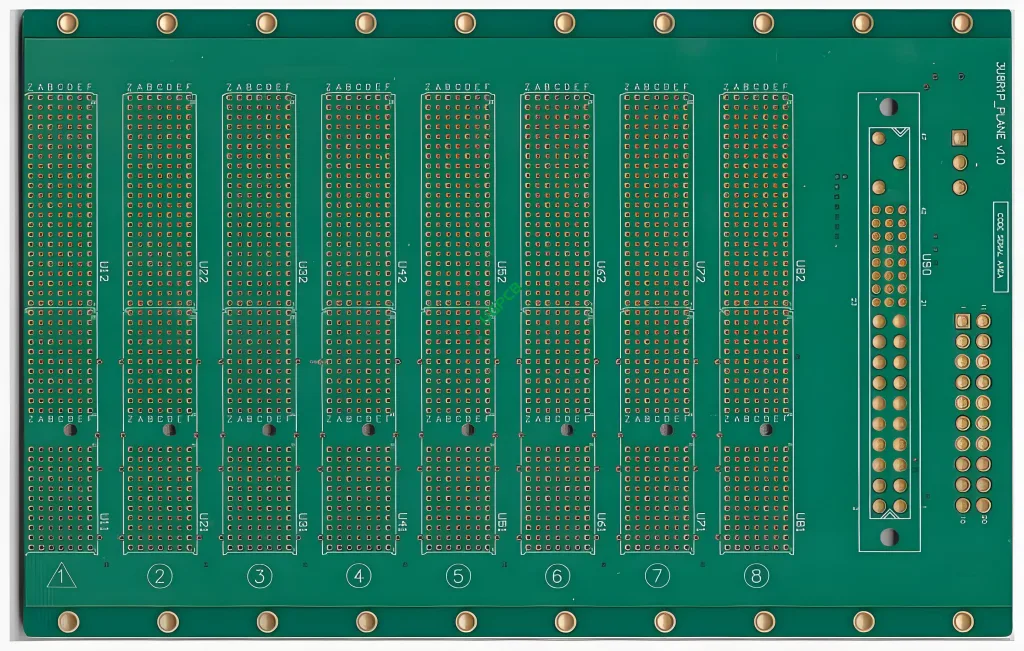
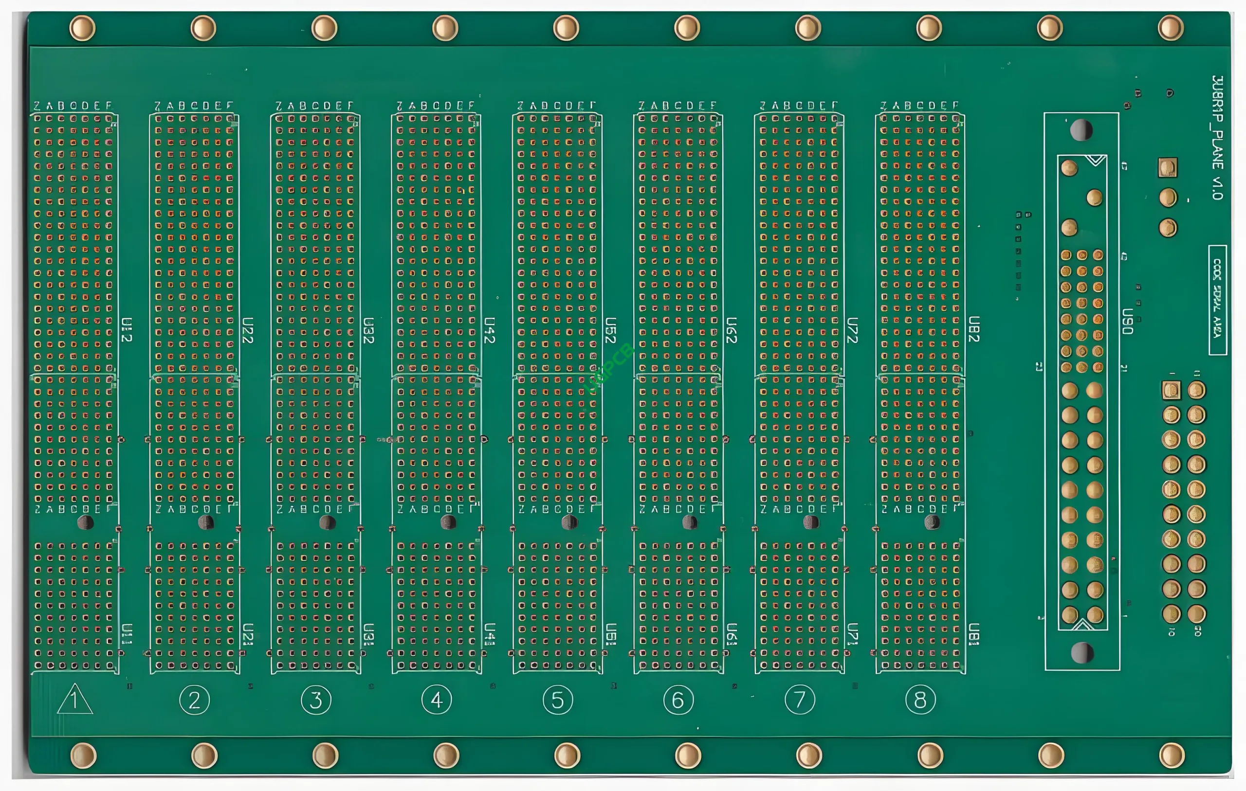
A 24 Layers Communication Backplane PCB refers to a multilayered printed circuit board that has been specifically designed with 24 layers of conductive material separated by dielectric layers. This structure allows for high-density interconnectivity while maintaining signal integrity and minimizing interference.
Entwurfsanforderungen
The design requirements for a 24 Layers Communication Backplane PCB are stringent due to its application in critical communication systems. Key design considerations include:
- Material: Panasonic M6, known for its excellent thermal and electrical properties.
- Schichtzahl: 24 layers to accommodate complex routing needs.
- Farbe: Blue/White for easy identification and aesthetic appeal.
- Fertige Dicke: 2.0mm to ensure structural integrity without being overly bulky.
- Kupferdicke: 1OZ to provide adequate conductivity.
- Oberflächenbehandlung: Eintauchen Gold, um die Lötlichkeit und Korrosionsresistenz zu verbessern.
Wie funktioniert es?
Der 24 Layers Communication Backplane PCB works by using multiple layers of copper traces separated by dielectric materials. These layers are interconnected through plated through-holes (PTHs) or vias, allowing signals to travel between different layers. The immersion gold surface treatment ensures that the copper traces remain conductive and resistant to oxidation.
Anwendungen
The primary application of the 24 Layers Communication Backplane PCB is in communication backplanes where high-speed data transmission and reliable connectivity are crucial. These PCBs are used in:
- Telecom infrastructure
- Data centers
- High-frequency communication devices
- Networking -Geräte
Einstufung
Basierend auf seinen Funktionen und Anwendungen, Die 24 Layers Communication Backplane PCB can be classified as a high-multilayer PCB. This classification highlights its capability to handle complex and dense circuit designs required for modern communication systems.
Materialzusammensetzung
The core material used in the 24 Layers Communication Backplane PCB is Panasonic M6, a high-performance laminate material known for its excellent mechanical, Thermal-, und elektrische Eigenschaften. This material ensures that the PCB can withstand the demands of high-speed communication applications.
Leistungseigenschaften
The performance characteristics of the 24 Layers Communication Backplane PCB include:
- Hohe Signalintegrität
- Niedriger Signalverlust
- Vorgesetzter thermisches Management
- Enhanced mechanical strength
- Reliable long-term stability
Strukturelle Details
The structural details of the 24 Layers Communication Backplane PCB are as follows:
- Schichtzahl: 24 Schichten
- Fertige Dicke: 2.0mm
- Kupferdicke: 1OZ
- Minimum Trace Width: 6Mil (0.15mm)
- Minimum Space Between Traces: 6Mil (0.15mm)
- Oberflächenbehandlung: Immersionsgold
Funktionen und Vorteile
The key features and benefits of the 24 Layers Communication Backplane PCB include:
- Interkonnektivität mit hoher Dichte
- Hervorragende Signalintegrität
- Robuste mechanische Konstruktion
- Zuverlässige langfristige Leistung
- Ästhetische Farboptionen (Blau/Weiß)
Produktionsprozess
The production process of the 24 Layers Communication Backplane PCB involves several steps, einschließlich:
- Materialauswahl: Choosing high-quality Panasonic M6 material.
- Schichtstapel: Arrangieren die 24 Schichten mit Präzision.
- Radierung: Entfernen Sie überschüssiges Kupfer, um die gewünschten Spurenmuster zu bilden.
- Überzug: Aufbringen von Einstimmungen Goldoberflächenbehandlung.
- Montage: Einbeziehung von PTHs und VIAS für Schichtverbindungen.
- Testen: Sicherstellen, dass die PCB alle Leistungsspezifikationen erfüllt.
Anwendungsfälle
Der 24 Layers Communication Backplane PCB is used in various scenarios, wie zum Beispiel:
- High-speed data transmission networks
- Telecommunication infrastructure projects
- Advanced networking equipment
- Data center applications requiring high bandwidth
Zusammenfassend, Die 24 Layers Communication Backplane PCB is a sophisticated and reliable component designed to meet the demanding requirements of modern communication systems. Its high-density design, excellent performance characteristics, and robust construction make it an essential part of any advanced telecommunication setup.


