
Understanding the 6Layers 1+N+1 Mobile Phone PCB
Product Overview
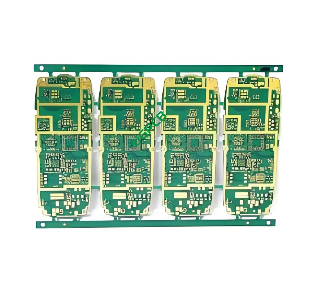
The 6Layers 1+N+1 Mobile Phone PCB represents an advanced electronic component tailored for integration into modern mobile devices. This PCB is characterized by its multi-layered structure, offering a balance between functionality and compactness essential for contemporary smartphones.
Definition
A Printed Circuit Board (Leiterplatte) is a foundational element in electronic devices, functioning as the platform that connects various electrical components. Der Begriff “6Layers 1+N+1” denotes a specific configuration within a PCB, indicating it consists of six layers, with the outermost layers dedicated to signal traces, power/ground planes, or a combination thereof, enhancing electrical performance and reducing signal interference.
Entwurfsanforderungen
Designing a 6Layers 1+N+1 Mobile Phone PCB entails adhering to stringent criteria:
- Material: S1000-2, chosen for its excellent thermal stability and mechanical strength.
- Dicke: A finished thickness of 0.8mm ensures compatibility with slim device profiles.
- Kupferdicke: Varies between inner 0.5OZ and outer 1OZ to manage heat dissipation and current-carrying capacity.
- Oberflächenbehandlung: Incorporates Immersion Gold and OSP (Organic Solderability Preservative) to enhance solderability and protect against corrosion.
Arbeitsprinzip
At its core, the PCB facilitates the flow of electrical signals between components. In a multi-layer design like the 6Layers 1+N+1, signal integrity is maintained through meticulous layer stacking, where ground planes can be interspersed between signal layers to minimize crosstalk and electromagnetic interference (EMI).
Anwendungen & Einstufung
Primarily designed for mobile phones, these PCBs are also suitable for other portable electronic devices requiring high-density interconnect solutions. They are classified based on their layer count, material properties, and intended use cases, making them versatile yet specialized for mobile technology.
Materialzusammensetzung
Constructed from S1000-2, a high-temperature epoxy resin glass cloth laminate, this PCB offers superior dimensional stability and durability under thermal stress, crucial for devices subject to varying environmental conditions.
Performance Features
- Signalintegrität: Maintains clear transmission of signals even at high frequencies due to optimized layer arrangement.
- Heat Dissipation: Efficient heat management thanks to copper thickness variations and material selection.
- Korrosionsbeständigkeit: Enhanced longevity through immersion gold and OSP surface treatments.
Structural Layout
The PCB’s structure comprises six layers, strategically arranged to optimize space usage and electrical performance. Der “1+N+1” configuration implies flexibility in assigning roles to each layer, typically involving signal layers sandwiched between power/ground planes.
Key Characteristics
- Slim Form Factor: With a thickness of just 0.8mm, it supports sleek device designs.
- High Density Interconnectivity: Supports complex circuitry with fine trace widths and spacing of 3mil/3mil.
- Robust Construction: Ensures durability and reliability in demanding mobile environments.
Produktionsprozess
Manufacturing involves several stages:
- Materialvorbereitung: Selecting premium S1000-2 substrate.
- Radierung: Creating precise circuit patterns using chemical etching processes.
- Layer Lamination: Bonding individual layers together under controlled pressure and temperature.
- Überzug: Applying copper layers to establish conductive paths.
- Oberflächenbehandlung: Applying Immersion Gold and OSP for protection and enhanced solderability.
- Qualitätskontrolle: Rigorous inspection and testing to ensure adherence to specifications.
Use Case Scenarios
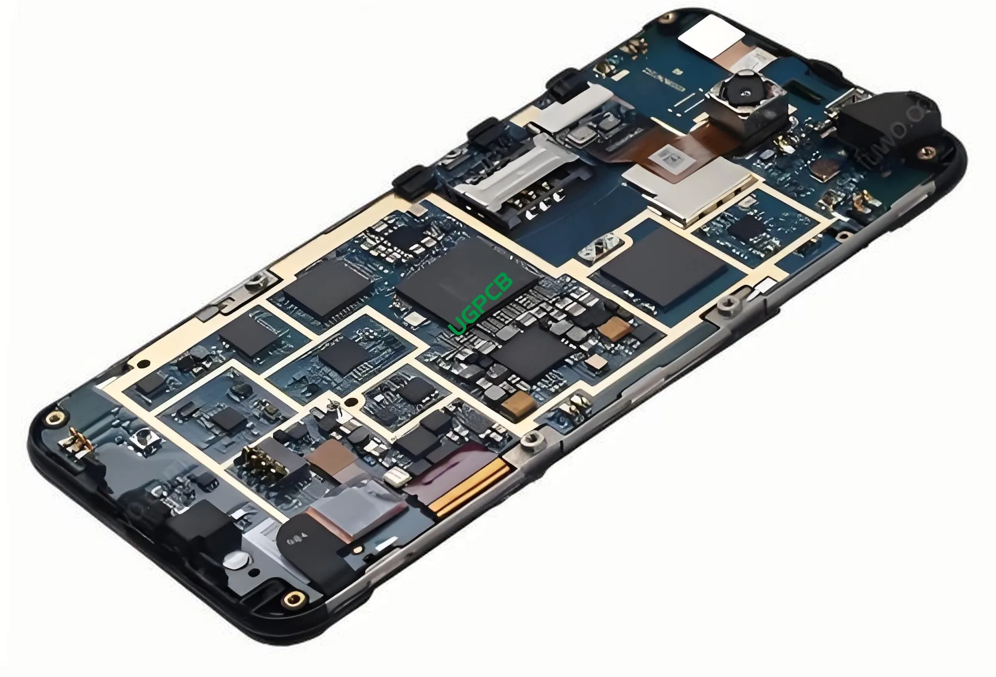
Ideal for high-performance mobile phones, the 6Layers 1+N+1 Mobile Phone PCB is also applicable in:
- Advanced smartphones with intricate circuit designs.
- Devices requiring miniaturization without compromising functionality.
- Applications needing reliable signal transmission and thermal management within compact spaces.
Zusammenfassend, the 6Layers 1+N+1 Mobile Phone PCB stands out as a sophisticated solution tailored for the demands of modern mobile electronics, offering unparalleled connectivity, durability, and performance within a minimalist form factor.


