
Jede Layer-HDI-Leiterplatte: Die komplexeste Designstruktur
Überblick
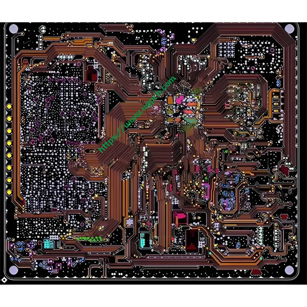
Jede Layer-HDI-Leiterplatte ist die komplexeste HDI-Leiterplatten-Designstruktur, bietet beispiellose Konnektivität und Leistung.
Verbindungsschichten mit hoher Dichte
Alle Layer als HDI
In dieser Struktur, Alle Schichten sind hochdichte Verbindungsschichten, Ermöglicht die freie Verbindung von Leitern auf jeder Schicht der Leiterplatte.
Kupfergefüllte gestapelte Microvia-Struktur
Die mit Kupfer gefüllte gestapelte Microvia-Struktur erleichtert diese Verbindung, Bereitstellung einer zuverlässigen und effizienten Möglichkeit zur Verbindung verschiedener Schichten.
Anwendungen
Hochkomplexe Geräte
Diese Struktur ist ideal für hochkomplexe, Geräte mit hoher Pinzahl wie CPU- und GPU-Chips, die in Handheld- und Mobilgeräten verwendet werden.
Hervorragende elektrische Eigenschaften
Das Design sorgt für hervorragende elektrische Eigenschaften, Damit es für Hochleistungsanwendungen geeignet ist.
Vorteile
Zuverlässige Verbindungslösung
Die Any-Layer-HDI-Leiterplattenstruktur bietet eine zuverlässige Verbindungslösung für komplexe Geräte, Gewährleistung einer stabilen und effizienten Leistung.
UGPCB -Vorteil
Diese Struktur, mit UGPCB-Technologie, stellt einen bedeutenden Fortschritt im PCB-Design und in der Herstellung dar.


