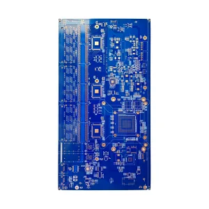
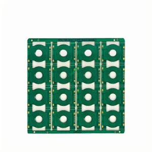
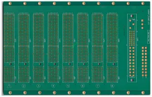
Produktübersicht
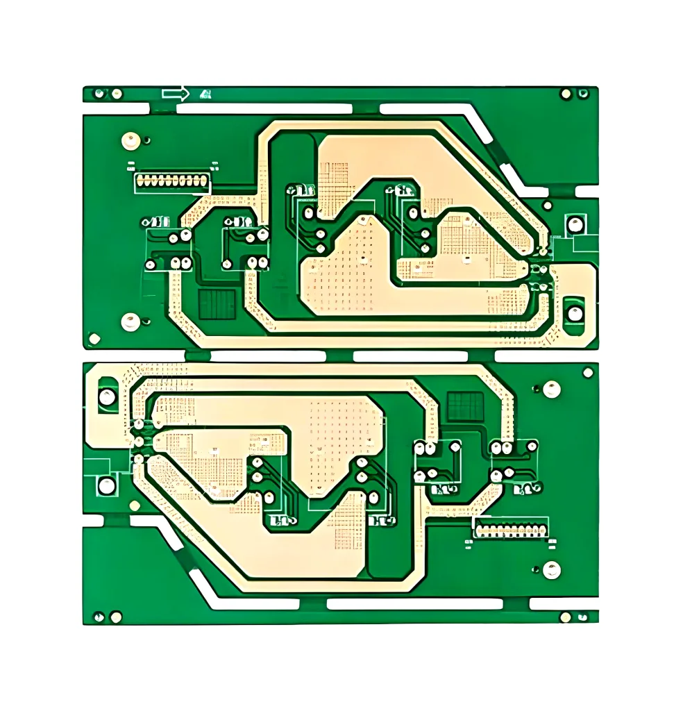
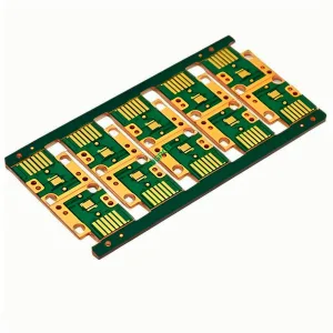
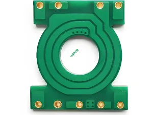
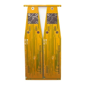
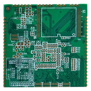
A 2-layer charging pile copper-based PCB is a circuit board used in charging piles, utilizing copper as the base material. It boasts excellent thermal conductivity and electrical performance. This circuit board is primarily used for the power module and control system within charging piles, providing stable power output and signal transmission functions.
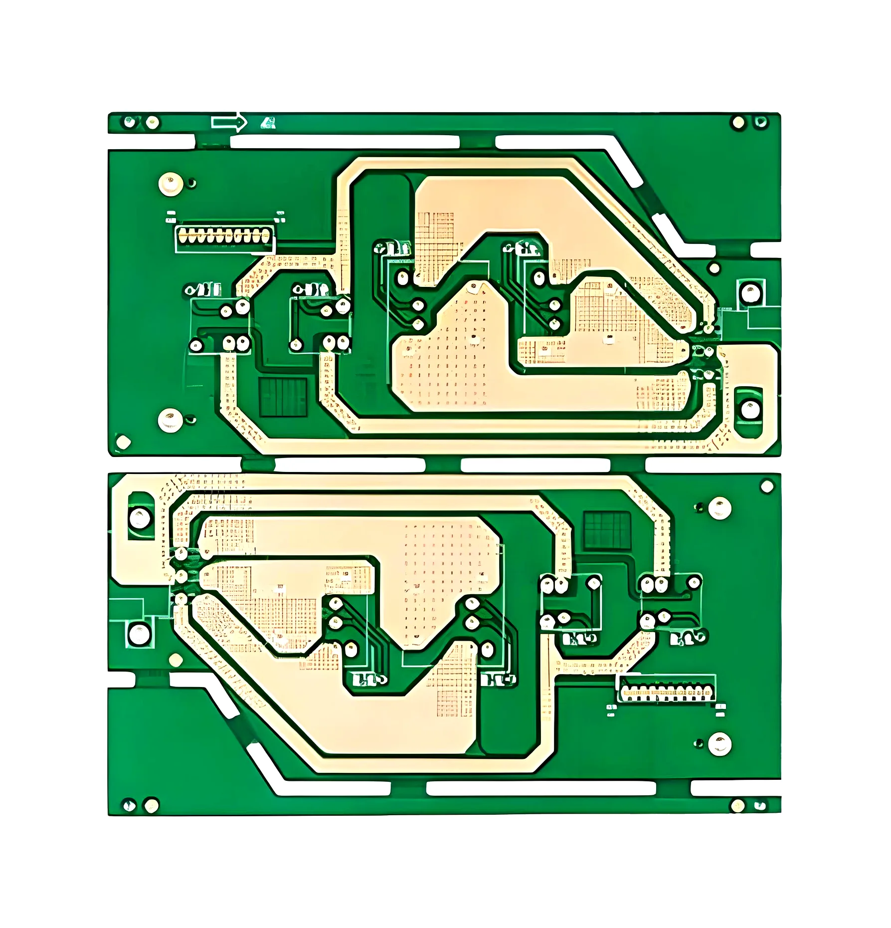
Charging pile copper-based PCB
Features of the 2-layer Charging Pile Copper-Based PCB
Good Thermal Conductivity
The copper base has good thermal conductivity, effectively dissipating heat generated within the charging pile to ensure its normal operation.
Ausgezeichnete elektrische Leistung
The copper base exhibits low resistivity and excellent conductivity, enabling stable power output and signal transmission.
Lightweight and Thin Design
The 2-layer charging pile copper-based PCB features a thin design, making it lightweight, compact, and easy to install and use.
Environmentally Sustainable
Made from eco-friendly materials and sustainable production processes, the copper base has minimal environmental impact and meets modern electronic product manufacturing’s environmental standards.
Efficient Production Process
Advanced manufacturing techniques allow for the rapid and precise production of 2-layer charging pile copper-based PCBs, enhancing production efficiency.
Cost-Effective
Compared to traditional PCB manufacturing technologies, copper-based PCBs can save on materials and reduce manufacturing steps, thereby lowering costs.
Wide Range of Applications
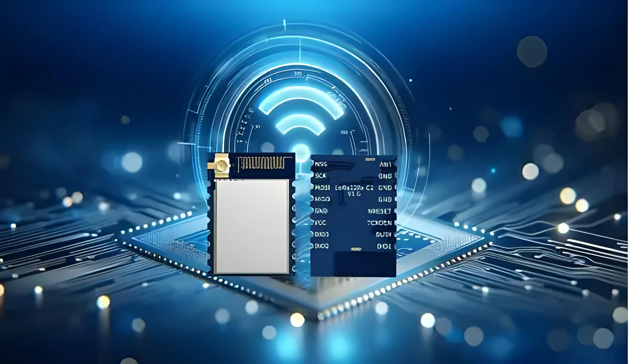
The application of PCB
The 2-layer charging pile copper-based PCB can be applied in various fields requiring excellent thermal conductivity and electrical performance, such as charging piles, power electronics, Telekommunikation, usw.
As a circuit board for charging piles, the 2-layer charging pile copper-based PCB offers excellent thermal and electrical properties, lightweight and thin design, environmental sustainability, efficient production process, Kosteneffizienz, and a wide range of applications, providing reliable support for the normal operation of charging piles.
Applications of Copper-Based PCBs
Hochfrequenzkreise
Copper-based PCBs have good thermal conductivity and electrical performance, suitable for heat dissipation and signal transmission in high-frequency circuits. Zum Beispiel, in the communication field, wireless communication devices like mobile phones, Bluetooth headsets, and wearables require copper-based PCBs to meet the demands of high-frequency signal transmission and heat dissipation.
High-Temperature and Humidity Environments
Copper-based PCBs have good high-temperature and humidity resistance, allowing stable operation in harsh environments, thus suitable for special fields such as automotive electronics and aerospace.
Leistungselektronik
With excellent thermal conductivity and electrical performance, copper-based PCBs are ideal for power modules and control systems in power electronics, offering stable power output and signal transmission functions.
LED-Beleuchtung
LED -Leuchten, characterized by their small size and high heat generation, require effective heat dissipation. Copper-based PCBs can meet these requirements while providing stable power output and signal transmission functions.
Andere Bereiche
Beyond the aforementioned areas, copper-based PCBs can also be applied in smart homes, medizinische Geräte, und anderen Bereichen, showcasing broad application prospects.
As an advanced circuit board technology, copper-based PCBs feature excellent thermal and electrical properties, high-temperature and humidity resistance, and are widely used in communications, Automobilelektronik, power electronics, LED lighting, und mehr.
 UGPCB-LOGO

