
Power Supply Flow and Filter Capacitor
After the power supply comes in, it goes to the filter capacitor first. After it comes out of the filter capacitor, it is sent to the back equipment. Because the wiring on the PCB board is not an ideal wire, there is resistance and distributed inductance. If the power is taken from the front of the filter capacitor, the ripple will be relatively large, and the filtering effect will be poor.
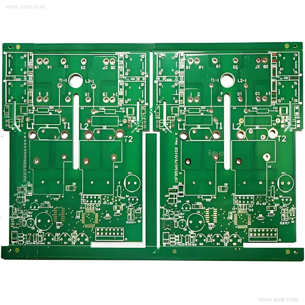
Line Layout Considerations
The line should be paid attention to: if it is possible to make a wide line, it must not be thin, there must be no sharp chamfering, and no right angle should be used for turning. The ground wire should be as wide as possible. It is better to use a large area of copper coating. This docking point problem has been greatly improved.
Capacitors for Filtering and Decoupling
Capacitors are set for switching devices (gate circuits) or other components that need filtering / decoupling. These capacitors should be arranged as close as possible to these components. If they are too far away, they will not work. When laying PCB (power board), the following safety regulations should be considered:
Safety Distances Before Fuse
The minimum safety distance between the two wires before the fuse and that between the two wires and the enclosure or internal grounding of the AC power supply line shall not be less than 6 mm, and the minimum safety distance between the two wires and the enclosure or internal grounding shall not be less than 8 mm.
Wiring Requirements After Fuse
Der Mindestkriechweg zwischen Null- und stromführenden Drähten darf nicht weniger als 3 mm betragen.
Kriechstrecke zwischen Hoch- und Niederspannungsbereichen
Der Mindestkriechweg zwischen Hochspannungsbereich und Niederspannungsbereich beträgt nicht weniger als 8 mm. Wenn es kleiner oder gleich 8 mm ist, A 2 Der Sicherheitsschlitz muss geöffnet sein.
Siebdruck für den Hochspannungsbereich
Der Hochspannungsbereich muss mit Hochspannungswarnschildern im Siebdruckverfahren versehen sein, d.h. Dreieckssymbole einschließlich Ausrufezeichen; Der Hochspannungsbereich ist mit Siebdruck zu umrahmen, und der Siebdruck der Rahmenstange darf nicht weniger als 3 mm betragen.
Sicherheitsabstand für Hochspannungsgleichrichterfilter
Der Mindestsicherheitsabstand zwischen Plus und Minus des Hochspannungsgleichrichterfilters beträgt nicht weniger als 2 mm. The design and development process is briefly described as follows:
Schematic Diagram
Make the schematic diagram according to the design.
Network Table
After the schematic diagram is compiled, the corresponding network table can be generated.
Keep Out Layer
Keep out layer is defined.
Introduction of Components and Networks
Components and networks are introduced.
Component Layout
The layout and routing of components have a great impact on the product life, stability, und elektromagnetische Verträglichkeit, which should be paid special attention to. Allgemein gesprochen, there should be some principles as follows:
- Placing sequence:
- Place the components related to the structure in fixed positions, such as power socket, indicator light, switch, Stecker, usw.
- Lock these devices with the lock function of software to prevent accidental movement.
- Place special components and large components on the circuit, such as heating elements, Transformatoren, IC, usw.
- Endlich, place small devices.
- Heat dissipation:
- Pay special attention to heat dissipation in the layout of components.
- For high-power circuits, place heating elements such as power tubes and transformers as far away as possible to facilitate heat dissipation.
- Avoid concentrating high capacitance too close to prevent premature aging of electrolyte.
Wiring
Wiring considerations for the PCB.
Adjustment and Perfection
After the wiring is completed, it is necessary to adjust the text, individual components, wiring, and copper (this work should not be too early, otherwise it will affect the speed and bring trouble to the wiring), which is also for the convenience of production, debugging, and maintenance. Copper coating usually refers to using large area copper foil to fill the blank area left after wiring. GND copper foil and VCC copper foil can be laid (but in case of short circuit, it is easy to burn the device, and it is better to ground it, unless it is used to increase the conduction area of power supply to bear large current before connecting VCC). Ground wrapping usually refers to wrapping a bunch of signal wires with special requirements by two ground wires (TRAC) to prevent it from being interfered or interfering with others. If copper is used instead of ground wire, attention must be paid to whether the whole ground is connected, the current size, flow direction, and whether there are special requirements, so as to reduce unnecessary errors.
Checking and Verifying the Network
Die Überprüfung und Verifizierung des Netzwerks führt manchmal aufgrund von Fehlbedienung oder Nachlässigkeit zu Abweichungen zwischen der Netzwerkbeziehung der gezeichneten Platine und dem Schaltplan, Daher ist es notwendig, das Netzwerk zu überprüfen. daher, nach dem Zeichnen, Beeilen Sie sich nicht zum Leiterplattenhersteller – UGPCB.


