
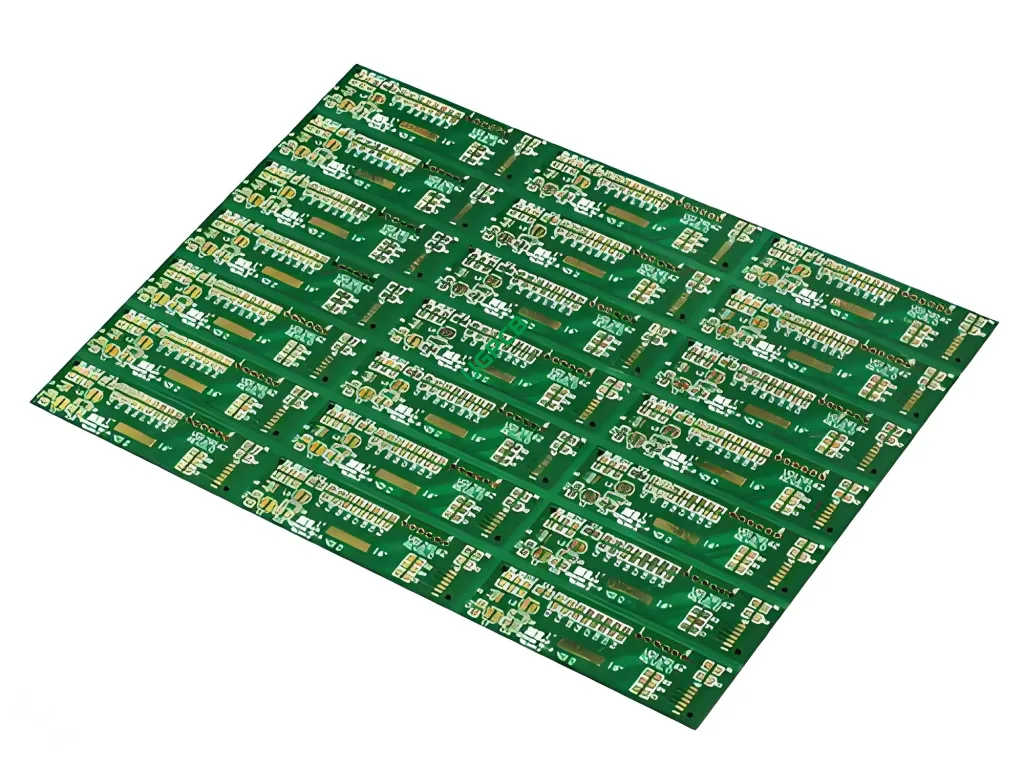
Overview of the P2.9 LED Printed Circuit Board
The P2.9 LED Printed Circuit Board (Leiterplatte) is a specialized PCB designed for use with P2.9 LED modules, which are commonly used in high-resolution display applications. This PCB is ideal for creating large, seamless LED displays.
What is a P2.9 LED Printed Circuit Board?
A P2.9 LED Printed Circuit Board is a printed circuit board (Leiterplatte) specifically designed to accommodate and connect P2.9 LED modules. Der Begriff “P2.9” refers to the pixel pitch of the LED module, which measures 2.9 millimeters between each pixel. This PCB ensures that the LED modules can be interconnected efficiently, providing a stable platform for the electronic components.
Entwurfsanforderungen
The design requirements for a P2.9 LED Printed Circuit Board are stringent to ensure its performance and reliability:
- Material: SY1000-2 TG170 FR4, Ausgewählt für seine hervorragenden elektrischen und thermischen Eigenschaften.
- Schichtzahl: 6 layers to accommodate the necessary circuitry and signal integrity.
- Farbe: Black/White for easy identification and aesthetic appeal.
- Fertige Dicke: 1.0MM zur Bereitstellung struktureller Integrität und Haltbarkeit.
- Kupferdicke: 1OZ, um eine angemessene Leitfähigkeit und Wärmeableitung zu gewährleisten.
- Oberflächenbehandlung: Eintauchen Gold, um die Lötlichkeit und Korrosionsresistenz zu verbessern.
- Mindestspur und Raum: 4Mil(0.1mm) Fine Schaltungsmuster zu unterstützen.
- Merkmal: More pads with small spacing to accommodate the dense layout of P2.9 LED modules.
Wie funktioniert es?
The P2.9 LED Printed Circuit Board works by providing a platform for various electronic components to be interconnected through conductive pathways. Diese Wege, oder Spuren, sind aus Kupfer und sind auf die Brett geätzt. The SY1000-2 TG170 FR4 material ensures that the PCB can withstand the demands of LED display applications, Während die Behandlung mit der Eintauchen Goldoberflächen sicherstellt, dass diese Spuren leitfähig und gegen Korrosion resistent bleiben.
Anwendungen
The primary application of the P2.9 LED Printed Circuit Board is in high-resolution LED display systems where it manages and regulates the flow of electrical signals. Dies schließt:
- Indoor and outdoor LED displays
- Digital signage
- Large format video walls
- Event stages and concert screens
Einstufung
Basierend auf seinen Funktionen und Anwendungen, the P2.9 LED Printed Circuit Board can be classified as a high-density, high-speed digital PCB designed for LED display applications. Diese Klassifizierung unterstreicht die Fähigkeit, Hochfrequenzsignale zu bewältigen und stabile elektrische Verbindungen bereitzustellen.
Materialzusammensetzung
The core material used in the P2.9 LED Printed Circuit Board is SY1000-2 TG170 FR4, Ein Hochleistungs-Verbundmaterial, der für seine hervorragende Mechanik bekannt ist, Thermal-, und elektrische Eigenschaften. This material ensures that the PCB can withstand the demands of LED display applications.
Leistungseigenschaften
The performance characteristics of the P2.9 LED Printed Circuit Board include:
- Hohe Signalintegrität
- Niedriger Signalverlust
- Vorgesetzter thermisches Management
- Robuste mechanische Stärke
- Langfristige Stabilität
Strukturelle Details
The structural details of the P2.9 LED Printed Circuit Board are as follows:
- Schichtzahl: 6 Schichten
- Fertige Dicke: 1.0mm
- Kupferdicke: 1OZ
- Oberflächenbehandlung: Immersionsgold
- Mindestspur und Raum: 4Mil(0.1mm)
- Merkmal: More pads with small spacing to accommodate the dense layout of P2.9 LED modules.
Funktionen und Vorteile
The key features and benefits of the P2.9 LED Printed Circuit Board include:
- Interkonnektivität mit hoher Dichte
- Hervorragende Signalintegrität
- Robuste mechanische Konstruktion
- Zuverlässige langfristige Leistung
- Ästhetische Farboptionen (Black/White)
Produktionsprozess
The production process of the P2.9 LED Printed Circuit Board involves several steps including:
- Materialauswahl: Choosing high-quality SY1000-2 TG170 FR4 material.
- Schichtstapel: Arrangieren die 6 Schichten mit Präzision.
- Radierung: Entfernen Sie überschüssiges Kupfer, um die gewünschten Spurenmuster zu bilden.
- Lötmaskenanwendung: Auftragen einer Lötmaskenschicht zum Schutz der Kupferspuren.
- Überzug: Aufbringen von Einstimmungen Goldoberflächenbehandlung.
- Montage: Einbeziehung von PTHs und VIAS für Schichtverbindungen.
- Testen: Sicherstellen, dass die PCB alle Leistungsspezifikationen erfüllt.
Anwendungsfälle
The P2.9 LED Printed Circuit Board is used in various scenarios such as:
- High-resolution indoor and outdoor LED displays
- Digital signage installations
- Concert and event stages with large video walls
- Retail environments with dynamic advertising screens


