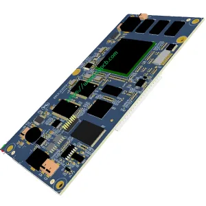
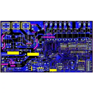
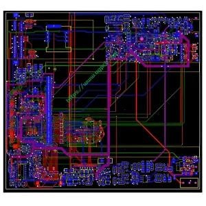
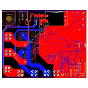
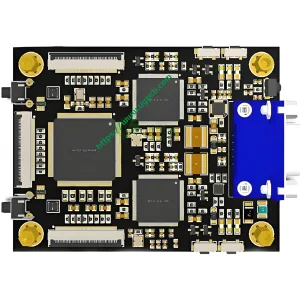
Overview of 4-Layer PCBs
A 4-layer PCB means that there are 4 layers to route electrical signals: top layer, inner layer 1, inner layer 2, and bottom layer.
Outer Layers: Arriba y Abajo
The top and bottom layers are the outer layers where components and wiring are placed.
Inner Layers: Inner 1 and Inner 2
Inner 1 and Inner 2 are located in the core and are typically used as power planes or for signal routing.
Configurations of 4-Layer PCBs
There are two common configurations for 4-layer PCBs:
Configuration 1: 3 Signal Layers + GND Layer
In this configuration, three of the layers are used for signal routing, and one layer is used as a ground (GND) plane.
Configuration 2: 2 Signal Layers + VCC Layer + GND Layer
In this configuration, two of the layers are used for signal routing, one layer is used as a power (VCC) plane, and one layer is used as a ground (GND) plane.
 UGPCB LOGO
