
Introducción
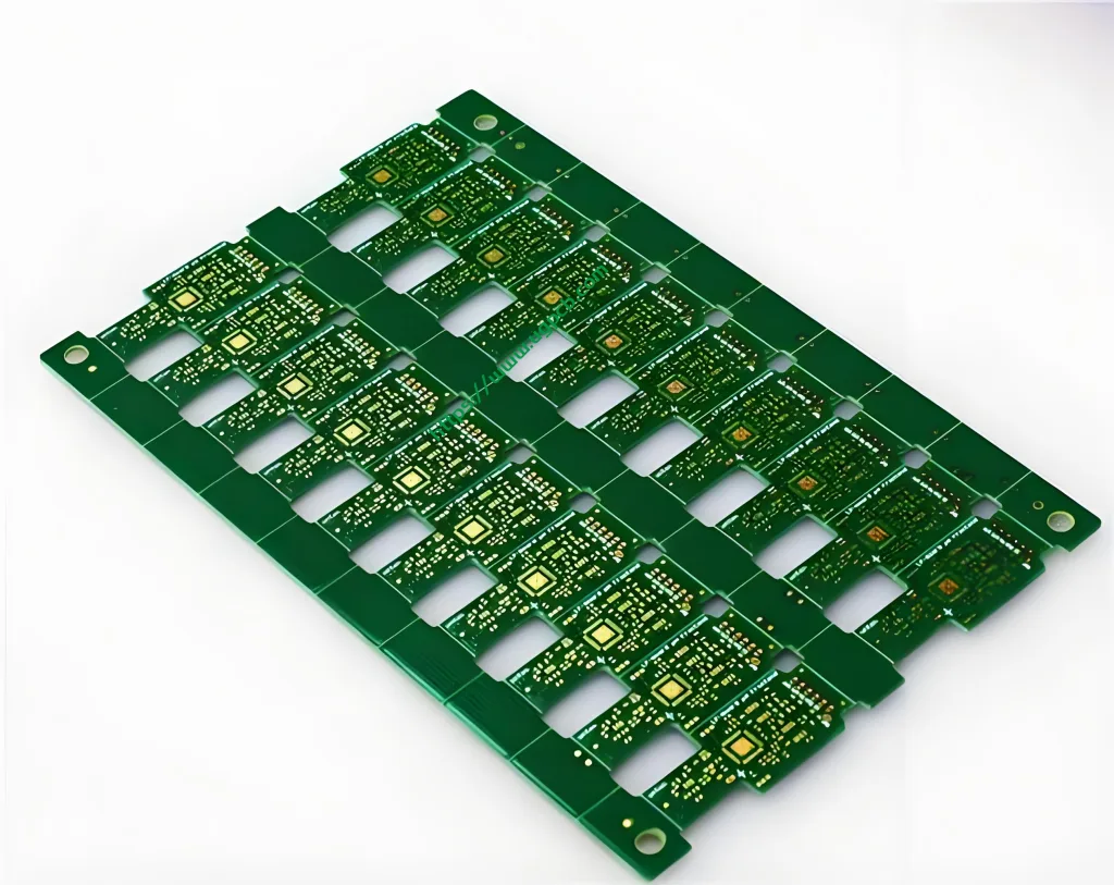
This is a mass production Double-side Printed Circuit Board (tarjeta de circuito impreso) that is maturely produced by UGPCB. We provide customers with low-cost PCBs and allow customers’ products to occupy the market.
Types of Double-sided PCBs
Double-sided Printed Circuit Board (tarjeta de circuito impreso) is a very important type of PCB. There are various types of double-sided PCBs available in the market, including double-sided circuit board metal base PCB, Hi-Tg heavy copper foil PCB, flat winding High-frequency double-sided PCB, PCB de alta frecuencia, hybrid dielectric base high-frequency double-sided PCB, etc.. These PCBs are suitable for a wide range of high-tech industries such as telecommunications, power supply, computadoras, controles industriales, digital products, scientific and educational equipment, equipo medico, automóviles, aeroespacial, etc..
Composition and Use
Double-sided Printed Circuit Board (tarjeta de circuito impreso) is usually made of epoxy glass cloth copper clad board. It is mainly used for communication electronic equipment, advanced instruments, and electronic computers with high performance requirements.
Proceso de producción
The production process of Double-sided Printed Circuit Board (tarjeta de circuito impreso) is generally divided into process wire method, hole blocking method, masking method, and pattern plating-etching method. The process flow of the pattern plating-etching method is commonly used.
Proofing and Finishing Processes

Double-sided Printed Circuit Board (tarjeta de circuito impreso) proofing is commonly done using craftsmanship. Además, processes such as the rosin process, OSP process, proceso de chapado en oro, immersion gold and silver plating processes are also applicable.
Specific Finishing Processes
Spray tin process: This offers a good appearance with a silver-white pad that is easy to tin and solder, and is cost-effective.
Sikkim process: This ensures stable quality and is usually used in cases involving bonding IC.
Circuit Layout
The difference between a double-sided Printed Circuit Board (tarjeta de circuito impreso) and a single-sided Printed Circuit Board (tarjeta de circuito impreso) is that the circuit of the single-sided PCB is only on one side of the PCB, while the double-sided PCB has circuits on both sides, connected through vias in the middle.
Production Parameters
The production of double-sided Printed Circuit Board (tarjeta de circuito impreso) differs from that of single-sided Printed Circuit Board (tarjeta de circuito impreso). In addition to the production process, there is an additional copper sinking process, which is the process of circuit conduction on both sides of the PCB.


