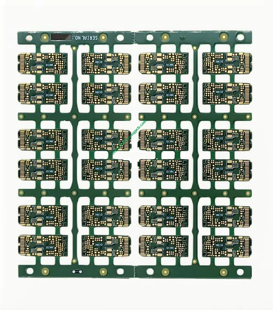
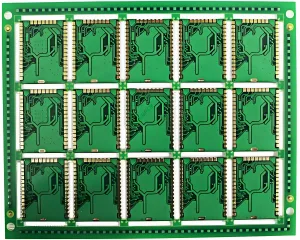
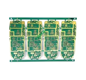
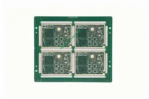
Introduction to Type-C Connector PCB
The Type-C Connector PCB is an advanced electronic component designed for high-speed data and power transmission. This guide provides a comprehensive overview of the product, including its definition, design requirements, working principles, uses, classifications, materiales, actuación, estructura, features, proceso de fabricación, and typical application scenarios.
Definición
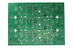
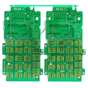
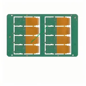
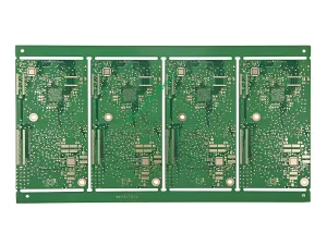
A Type-C Connector PCB (Placa de circuito impreso) is a specialized circuit board that incorporates a USB Type-C connector. It is designed to support high-speed data transfer and power delivery, making it ideal for modern electronic devices.
Design Requirements
The design of a Type-C Connector PCB must adhere to specific standards to ensure optimal performance and reliability. Key design requirements include:
High-Speed Data Transmission
Supports USB 3.1 Gen 2 or higher standards for fast data transfer rates.
Power Delivery
Capable of handling up to 100W of power delivery, suitable for charging and powering devices.
Minimal Trace/Space
Ensures fine pitch components can be placed accurately with a minimum trace/space of 3mil/3mil.
Precision Tolerances
Maintains strict tolerance requirements for outline and PSR (Pick and Place Reliability).
Principio de trabajo
The Type-C Connector PCB operates based on the principles of electrical conductivity and signal integrity. It utilizes copper traces embedded in a high TG FR4 substrate to transmit signals between the Type-C connector and other electronic components on the board. The immersion gold and OSP surface treatments enhance conductivity and protect against oxidation.
Uses
Type-C Connector PCBs are used in a variety of applications where high-speed data transfer and power delivery are essential. Common uses include:
Data Transfer
Facilitates quick and efficient data transfer between devices such as laptops, teléfonos inteligentes, and external storage devices.
Power Supply
Provides reliable power delivery for charging batteries and powering electronic devices.
Device Connectivity
Enables connectivity between various devices, enhancing the functionality and versatility of electronic systems.
Classifications
Type-C Connector PCBs can be classified based on several criteria:
By Layer Count
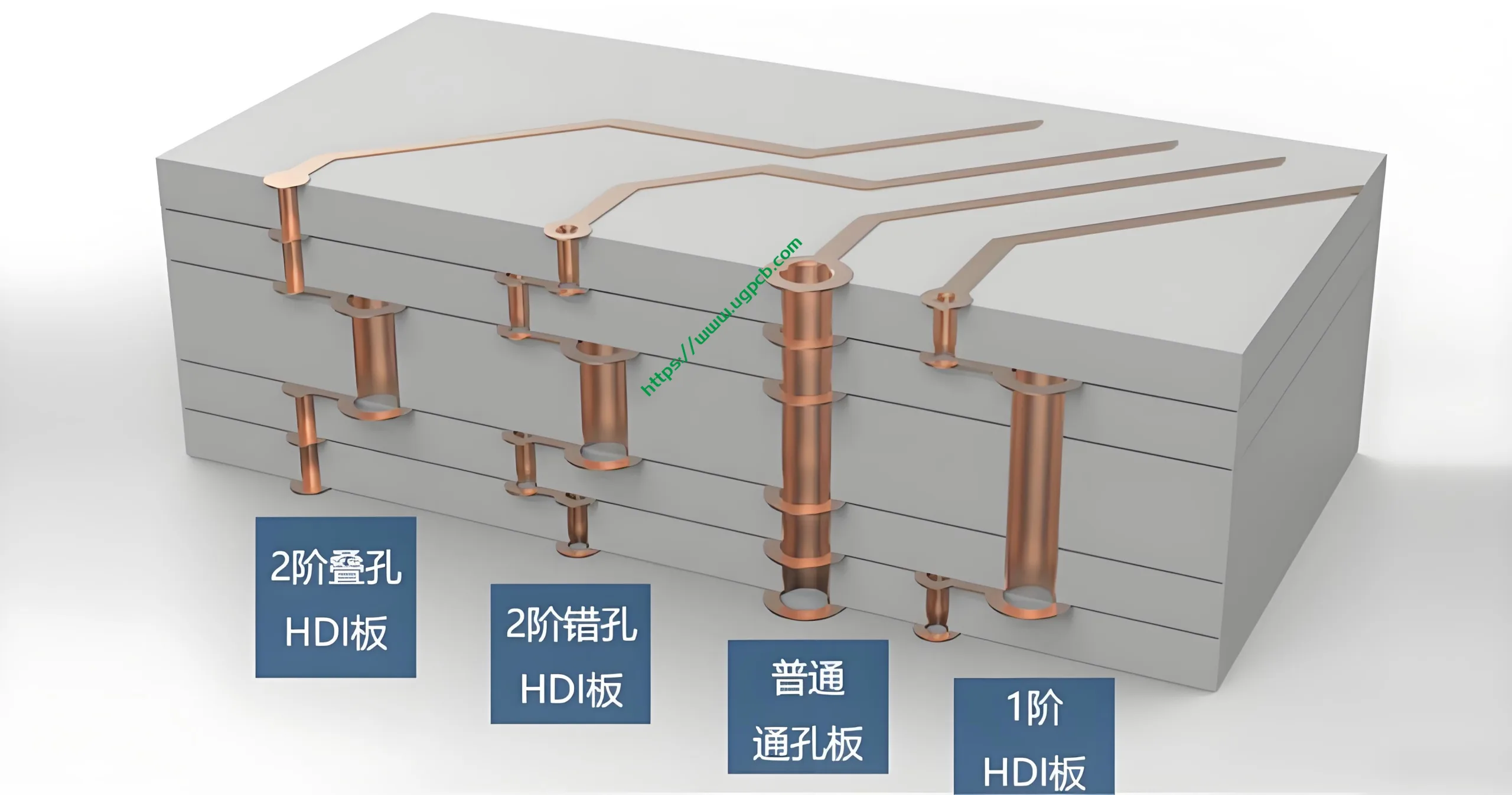
Multi-layer PCBs, such as the 6-layer HDI (High Density Interconnect) PCB mentioned.
By Material
Constructed from high TG FR4 material for enhanced thermal stability.
By Surface Treatment
Features immersion gold and OSP (Organic Solderability Preservative) surface treatments for improved conductivity and durability.
Materiales
The primary materials used in the construction of Type-C Connector PCBs include:
High TG FR4
A flame-retardant glass-reinforced epoxy laminate material known for its high thermal stability and mechanical strength.
Cobre
Used for the conductive traces, with a standard thickness of 1OZ.
Green/White Color (PSR: TAIYO INK)
The color of the PCB, achieved using TAIYO INK for consistent and vibrant results.
Performance
The performance of Type-C Connector PCBs is characterized by:
High Signal Integrity
Ensures minimal loss of signal quality over long distances and high frequencies.
Durabilidad
Resistant to environmental factors such as temperature variations and humidity.
Fiabilidad
Designed to withstand repeated connections and disconnections without degradation.
Structure
The structure of a Type-C Connector PCB typically includes:
Multi-Layer Design
A 6-layer HDI PCB with 2+N+2 layer configuration for complex circuitry.
Fine Pitch Components
Allows for the integration of fine pitch components with a minimum hole size of 0.2mm for mechanical holes and 0.1mm for laser holes.
Advanced Surface Treatments
Immersion gold and OSP coatings enhance conductivity and protect against corrosion.
Características
Key features of Type-C Connector PCBs include:
High-Speed Data and Power Transmission
Supports USB 3.1 Gen 2 or higher standards for rapid data transfer and up to 100W power delivery.
Diseño compacto
Slim profile with a finished thickness of 0.8mm, suitable for slim and sleek device designs.
Robust Construction
Made from high TG FR4 material for enhanced durability and thermal stability.
Proceso de producción
The production of Type-C Connector PCBs involves several steps:
Preparación de material
Selection of high TG FR4 material and copper sheets.
Apilamiento de capas
Stacking of multiple layers to form a multi-layer PCB.
Perforación
Creation of holes for through-hole components and vias using mechanical and laser drilling techniques.
Enchapado
Application of copper plating to create conductive paths.
Aguafuerte
Removal of excess copper to form the desired circuit pattern.
Tratamiento superficial
Application of immersion gold and OSP coatings for improved conductivity and protection.
Typical Application Scenarios
Type-C Connector PCBs are widely used in various applications, incluido:
Electrónica de Consumo
Smartphones, tabletas, computadoras portátiles, y otros dispositivos portátiles.
Automotive Industry
In-car entertainment systems and charging solutions.
Equipos industriales
Control panels and communication devices requiring robust connectivity.
By understanding these aspects, you can appreciate the versatility and importance of Type-C Connector PCBs in modern electronic design.
 UGPCB LOGO

