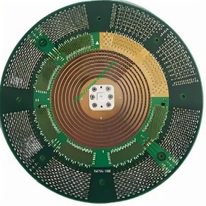
Composición de materiales
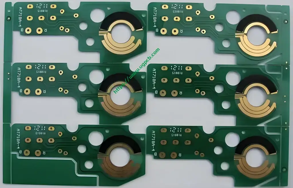
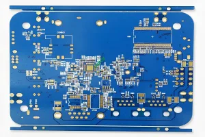
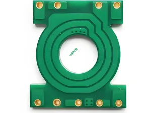
The Laser repair of carbon film PCB is crafted using FR-4 as its foundational material, reinforced with a layer of carbon film PCB. This combination ensures a sturdy and reliable base for the electronic components.
Especificaciones de rendimiento
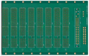
The PCB boasts a 2-layer design, with a copper thickness of 1OZ, contributing to its electrical conductivity. The finished thickness of 1.0mm provides a balanced mix of durability and compactness. The surface treatment of Immersion Gold enhances its corrosion resistance and ensures better soldering performance.
Design Characteristics
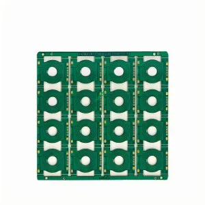
The trace and space of 6mil/6mil allow for intricate circuit designs while maintaining electrical isolation. With a minimum hole size of 0.3mm (12mil), it supports the integration of fine components. A unique aspect of this PCB is the printing of carbon film and the special process of laser repair resistance value, ensuring high precision and accuracy in resistance settings.
Production Workflow
The production of the Laser repair of carbon film PCB involves a series of well-defined steps. Initially, the FR-4 base material is prepared. Después, the carbon film is precisely printed onto the surface. After this, the copper layer is added and etched to form the circuits according to the specified trace/space. The immersion gold surface treatment is then applied. Finalmente, the laser repair process is carried out to adjust and finalize the resistance values, ensuring each PCB meets the required specifications.
Escenarios de aplicación
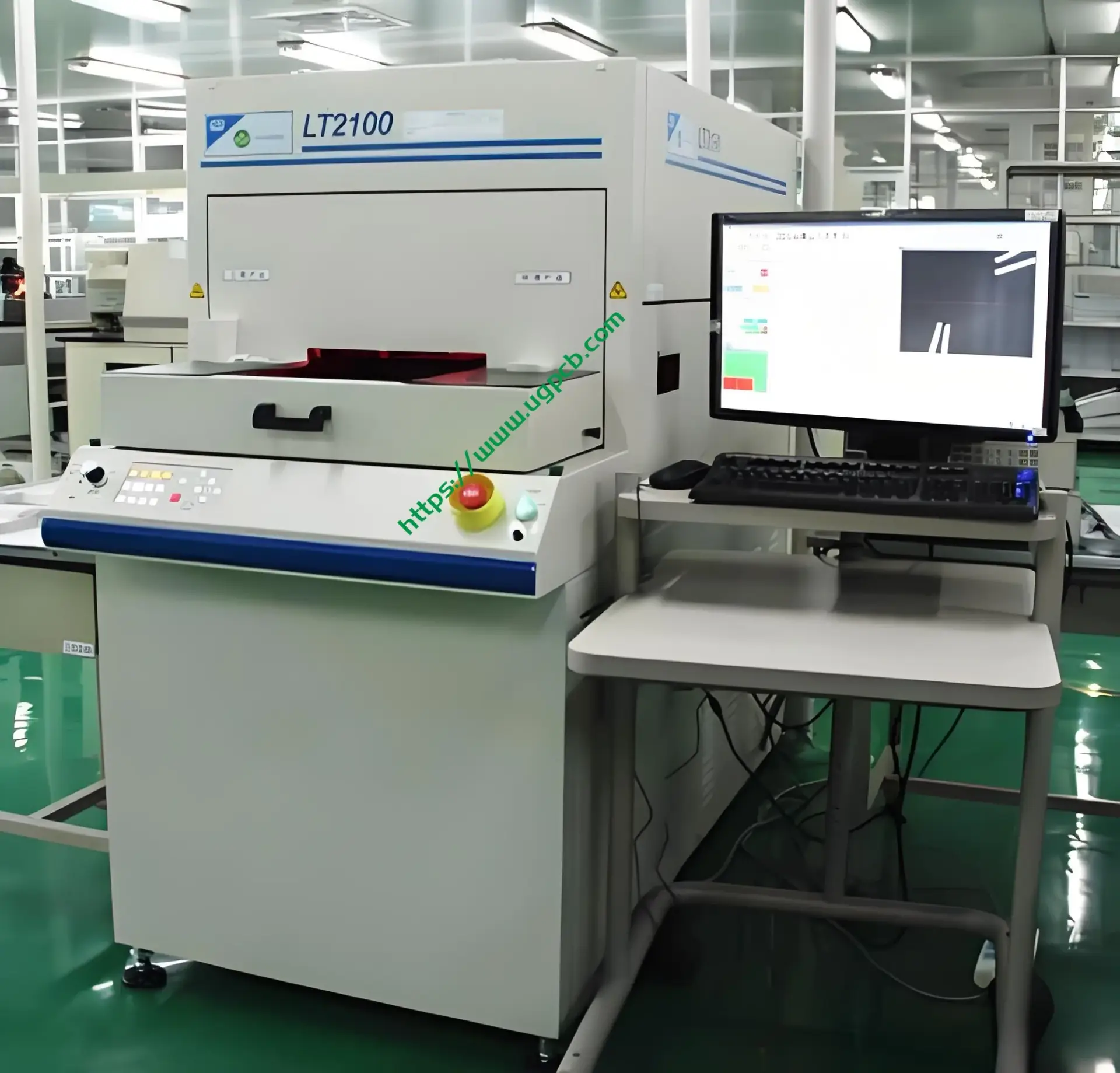
This versatile PCB finds its application in various high-performance electronic devices. It is ideal for RF isolator PCBs, RF circulator PCBs, RF resistor PCBs, and terminal load PCBs. Its precise resistance adjustment capabilities make it perfect for attenuation chip PCBs, coaxial attenuator PCBs, and filter PCBs. It is also suitable for combiner PCBs, duplexer PCBs, power divider PCBs, waveguide series PCBs, and antenna PCBs. Essentially, wherever high precision and reliability are paramount, the Laser repair of carbon film PCB shines.
With its robust material composition, precise performance specifications, unique design characteristics, well-structured production workflow, and versatile application scenarios, the Laser repair of carbon film PCB stands out as a reliable choice for modern electronics.
 UGPCB LOGO

