Introduction to New Energy Vehicle PCB
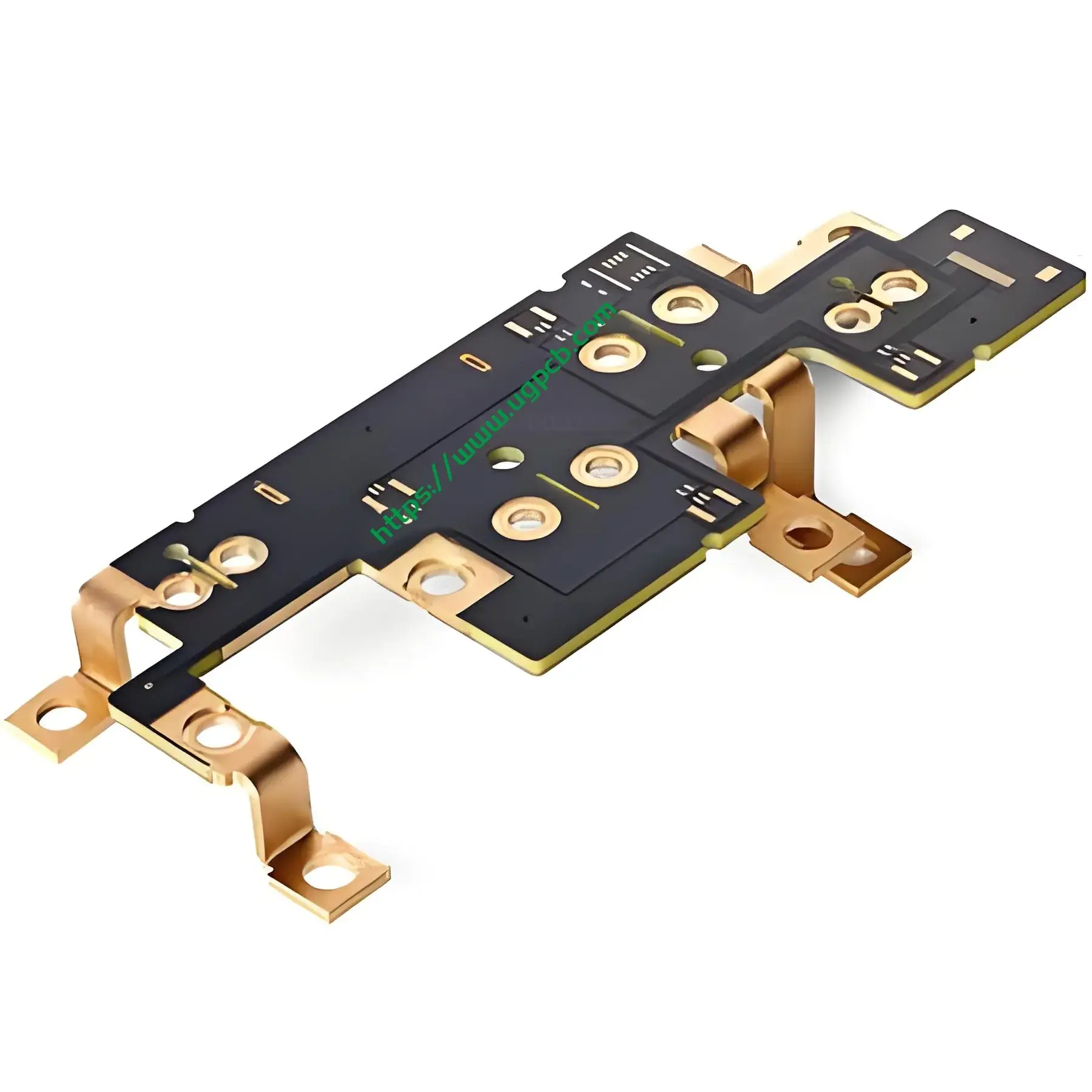
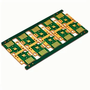
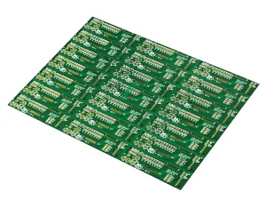
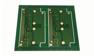
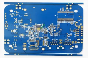
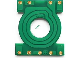
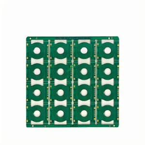
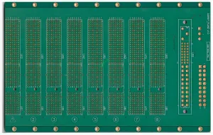
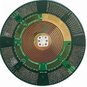
The New Energy Vehicle PCB is a cutting-edge product designed to meet the high-performance demands of modern electric and hybrid vehicles. This advanced printed circuit board (tarjeta de circuito impreso) integrates innovative materials and manufacturing techniques to ensure reliability, eficiencia, and durability in automotive applications. Below is a comprehensive overview of its material composition, performance characteristics, unique features, proceso de producción, and typical usage scenarios.
Composición de materiales
The New Energy Vehicle PCB is crafted from high-quality materials that guarantee its robustness and functionality. It features a 4-layer design with a plate thickness of 5.0mm, offering excellent structural support and electrical insulation. The inner copper thickness of 3.0mm ensures efficient heat dissipation and current carrying capacity, while the outer copper thickness of 1oz (approximately 35µm) provides good conductivity and solderability.
Características de rendimiento
This PCB excels in its precision and reliability. With a minimum aperture of 1.0mm and a minimum line width/distance of 0.5/0.27mm, it supports complex circuit layouts and high-density interconnectivity. The surface treatment, Electroless Nickel Immersion Gold (ACEPTAR), enhances corrosion resistance and solderability, ensuring long-term reliability in harsh environments.
Unique Features
One of the notable features of the New Energy Vehicle PCB is its controlled depth milling and bending capabilities. This allows for precise positioning of components and the creation of intricate shapes without compromising the structural integrity of the board. Además, the minimum distance from hole to line is carefully controlled to prevent electrical shorts and ensure optimal performance.
Proceso de producción
The production of the New Energy Vehicle PCB involves several meticulous steps:
- Preparación de material: High-quality copper-clad laminates are selected based on their electrical and mechanical properties.
- Patrón de circuito: Using advanced photolithography techniques, the circuit patterns are etched onto the copper surface.
- Enchapado: An ENIG surface finish is applied to enhance corrosion resistance and solderability.
- Drilling and Milling: Precision drilling and controlled depth milling are performed to create through-holes and intricate features.
- Bending and Assembly: The PCB is bent to the required shape, and components are assembled using automated processes.
- Control de calidad: Rigorous testing is conducted to ensure the PCB meets all specified performance criteria.
Escenarios de uso
The New Energy Vehicle PCB finds application in a wide range of electric and hybrid vehicles. It is ideal for use in power management systems, battery management units, motor controllers, and other critical automotive electronics. Its high-performance characteristics make it suitable for use in high-voltage and high-current environments, ensuring reliable operation and enhanced safety.
En conclusión, the New Energy Vehicle PCB is a sophisticated and reliable component that plays a vital role in the operation of modern electric and hybrid vehicles. Its innovative design and meticulous manufacturing process ensure it meets the stringent demands of automotive applications, providing efficient, durable, and safe performance.
 UGPCB LOGO


