Overview of RF PCB Design
Introduction to RF PCB Design
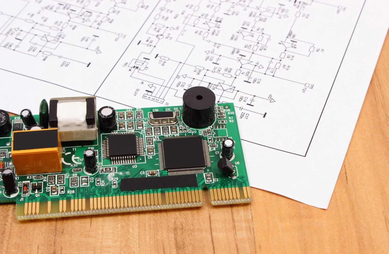
In the wireless communication system, only a small part of the front-end circuit works in the radio frequency stage, which is commonly known as the radio frequency front-end circuit. The rest of the circuit is used for low frequency baseband analog and digital signal processing. RF front-end circuits generally include low-noise amplifiers, mixers, and power amplifiers. Although the number of components in this part of the circuit is much less than that of the baseband circuit, it is still the key to the success or failure of the entire system.
Key Metrics and Design Challenges
Similar to the octagon rule for analog IC design, RF PCB design requires analog signal processing at wide dynamic range and high frequencies. Por lo tanto, RF PCB design also has its own hexagon rule. Noise, linearity, supply voltage, gain, operating frequency, and power are the most important metrics in an RF PCB. In practical designs, any two or more of these parameters will constrain each other, resulting in multidimensional optimization problems. Such compromises and mutual constraints bring many problems to the design of RF PCBs. Often, it takes the intuition and experience of the RF designer to arrive at a better compromise.
Application Fields of RF PCB
Various Applications of RF PCB
- Base Station RF Circuit Board
- Mobile Phone RF Circuit Board
- Wireless Local Area Network (WLAN) Placa de circuito impreso RF
- Sistema de posicionamiento global (GPS) RF Circuit Board
- Radio Frequency Tag (RFID) Placa de circuito impreso RF
- Internet de las cosas (IoT) Placa de circuito impreso RF
 UGPCB LOGO
