PCB Wiring Considerations
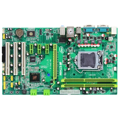
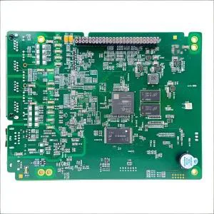
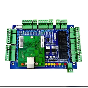
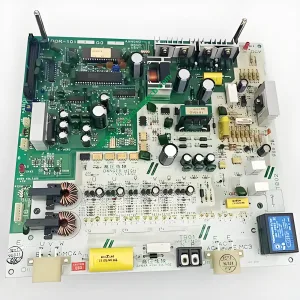
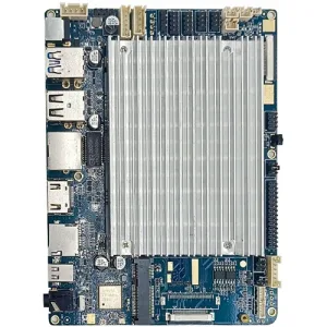
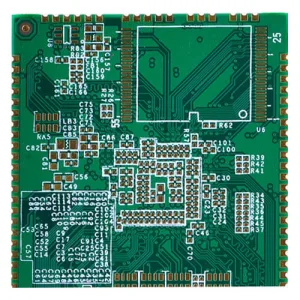
For SMT small-batch patch processing, there are numerous factors to consider in PCB wiring. Merely using automatic wiring tools is insufficient to achieve the desired effect. This is due to various factors such as PCB production costs, electromagnetic interference between components, and aesthetics.
General Principles
Although there is no universal standard, some generally applicable principles exist for SMT patch proofing:
- Cross-talk Prevention: For double-sided or multi-layer boards, the lines on both sides should be perpendicular to prevent mutual induction-induced crosstalk.
- Wiring Priority: Prioritize key signal lines such as power supply, analog small signal, high-speed signal, clock signal, and synchronization signal.
- Ground Wire Separation: For high-current devices like relays, indicator lights, and speakers, separate ground wires to reduce noise.
- Weak Signal Line Protection: If there is a small signal amplifier, keep the weak signal line before amplification away from strong signal lines. Shield with a ground wire if possible.
- Signal Line Spacing: Leave a large gap between parallel signal lines to reduce interference. Insert a grounding line between close signal lines for shielding.
- Transmission Line Design: Avoid excessive steering angles in signal transmission lines to prevent reflections. Consider designing uniform arc lines or obtuse angles.
Component Layout Requirements
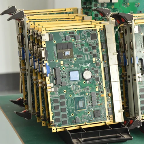
PCBA small-batch proofing has specific requirements for the component layout of SMT patch processing. Reasonable layout planning enhances the processing and production process.
Key Considerations
- Replaceable and Adjustable Components: Place frequently replaced or adjusted components in easily accessible locations.
- Temperature-Sensitive Components: Keep temperature-sensitive components away from heating components and high-power devices.
- Arrangement Direction: Maintain consistency in the arrangement direction of SMD components for ease of mounting, welding, y pruebas.
- Balanced Distribution: Distribute high-quality SMT components evenly to avoid local temperature differences and virtual soldering issues.
- Heating Components: Place heating components in corners and ventilation positions for efficient heat dissipation. Ensure they are supported and maintain a distance of at least 2mm from the PCB surface.
Small Batch PCB Assembly Patch Services
UGPCB supports small batch PCB assembly patch business. Somos una fábrica profesional de ensamblaje integral de PCBA.. Bienvenido a hacer un pedido.
 UGPCB LOGO

