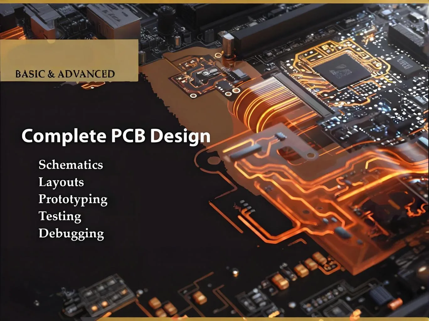
L'art et la science de la conception de PCB: Comment l'UGPCB maîtrise l'alchimie des circuits imprimés
(Excellence en ingénierie du PCBA schématique au PCBA fonctionnel)
Un simple via égaré sur une carte mère de serveur à 12 couches a déjà coûté un géant de la technologie $2.3 millions de rappels. Au Shenzhen R de l'UGPCB&Centre D, les ingénieurs scrutent à travers des caméras thermiques haute résolution, ajuster les largeurs de trace avec une précision micrométrique pour éviter de telles catastrophes.
Avec plus 2000+ annuel Conception de circuits imprimés projets dans l'aérospatiale, médical, et les secteurs 5G, UGPCB transforme les schémas conceptuels en chefs-d'œuvre réalisables. Leur secret? Une fusion de 10+ années d'expertise et des protocoles de conception de qualité militaire qui permettent taux d'échec zéro dans les applications critiques.
1. L’impératif stratégique: Pourquoi la conception de circuits imprimés dicte le succès d'un produit
Dans 2024, 68% des pannes de produits électroniques remonte à Disposition des circuits imprimés défauts (Rapport IPC). La philosophie de conception de l'UGPCB considère les circuits imprimés comme sculptures fonctionnelles où:
-
Chaque coin de trace à 90 ° augmente l'EMI de 3-5db
-
0.1mm via un désalignement peut dégrader les signaux 56 Gbps de 40%
-
Une conception thermique appropriée prolonge la durée de vie des composants de 2.3X
“La conception de PCB ne consiste pas à tracer des lignes, mais à orchestrer des autoroutes électroniques”
— Ingénieur de conception principal de l'UGPCB
L'impact économique est stupéfiant:
-
DFM (Conception pour la fabrication) l'intégration réduit les coûts de prototypage en 65%
-
Tôt simulation de l'intégrité du signal coupe les relances de 80%
-
Les modèles de stackup standardisés de l’UGPCB accélèrent la mise sur le marché en 4 semaines
2. L'avantage UGPCB: L'ADN de l'ingénierie décodé
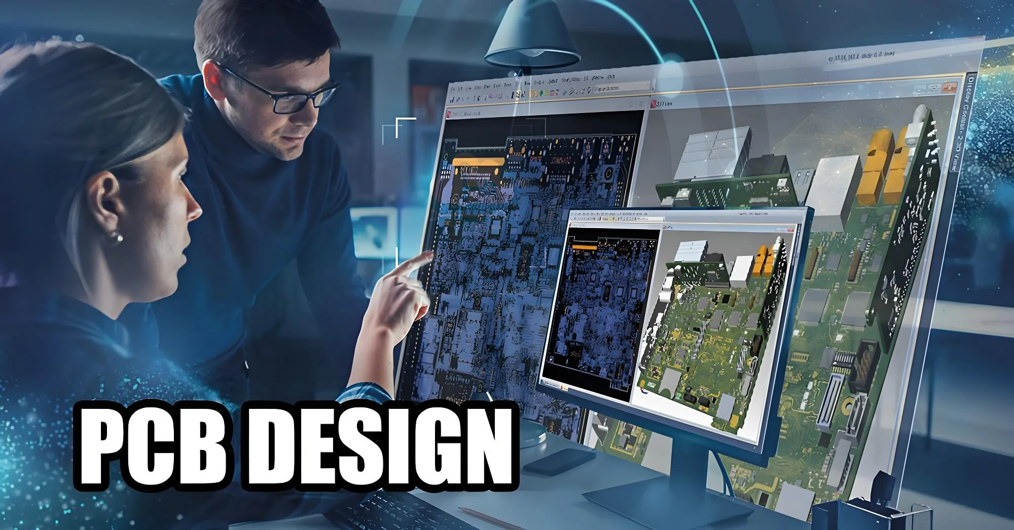
2.1 Écosystème de conception conçu avec précision
UGPCB workflow de triple vérification établit des références dans l'industrie:

Spécialisation matérielle:
-
56Gbit/s PAM4 conceptions de fond de panier
-
0.2Pitch MM Routage BGA
-
20+ couche Cartes HDI avec 0.1Microvias MM
-
RF vers numérique mises en page hybrides (6GHz+)
2.2 Arsenal d’outils de pointe
| Logiciel | Capacités | Mise en œuvre de l'UGPCB |
|---|---|---|
| Cadence SPB 16.6 | 3Simulation EM, routage piloté par les contraintes | Conceptions de cartes mères de serveur |
| Concepteur avancé 23 | Intégration ECAD/MCAD unifiée | Dispositifs médicaux portables |
| Siemens Expédition | Planification de système multi-cartes | Unités de contrôle automobile |
| IA thermique propriétaire | Cartographie prédictive des points chauds | Contrôleurs industriels haute puissance |
3. L'alchimie de la transformation des circuits: Processus de conception de l’UGPCB
3.1 Phase d’incubation de concepts
-
Déconstruction des exigences: Convertir les spécifications du client en 23-matrices techniques ponctuelles
-
Analyse de faisabilité: Recoupez-vous avec CIB-2221 normes
-
Plan d’atténuation des risques: Drapeau 97% des problèmes de fabricabilité
3.2 Magie de synthèse schématique
Les ingénieurs de l’UGPCB tirent parti:
-
Base de données d'intelligence des composants: 500k+ empreintes vérifiées
-
Contrôle de l'impédance Formules:

(Réalisable via les UGPCB 13-bibliothèque d'empilement de couches)
-
Modélisation de l'intégrité de l'alimentation:

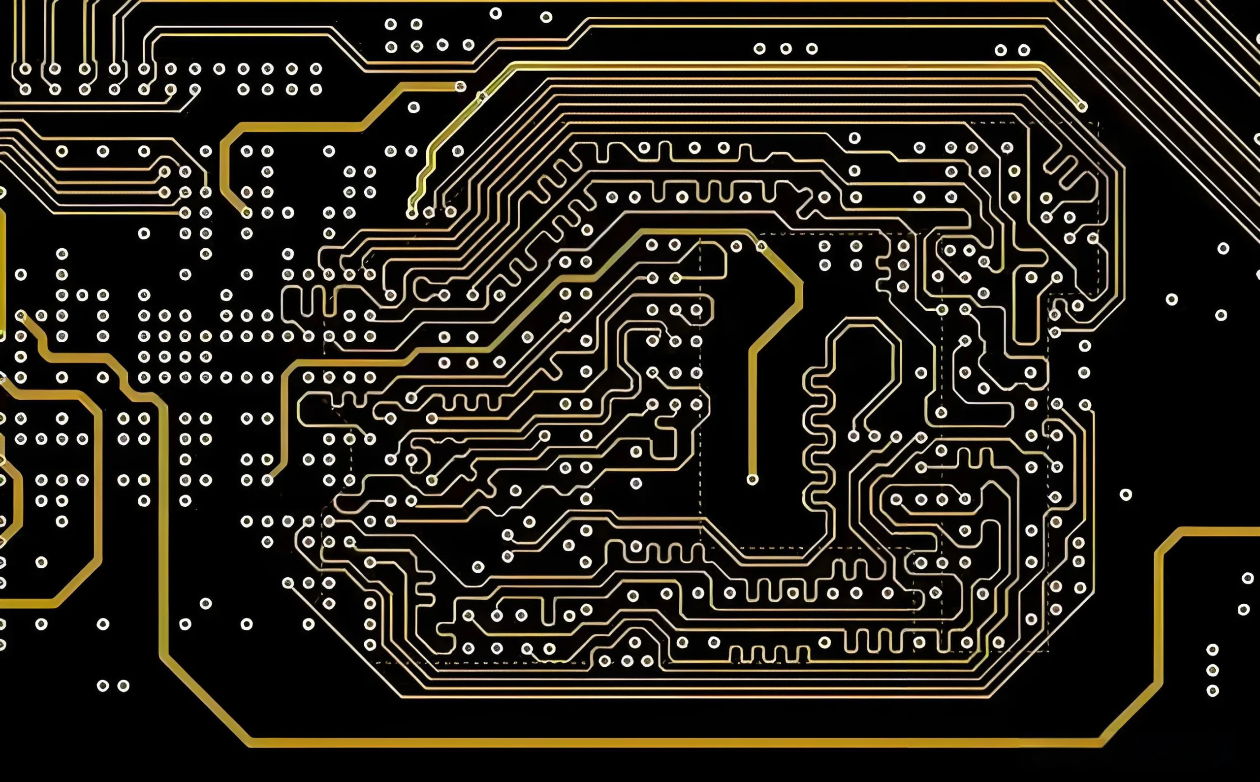
3.3 Chorégraphie de mise en page
Règles critiques appliquées:
-
3Principe W: Espacement des traces = 3× largeur de trace pour le contrôle de la diaphonie
-
10° Règle: Éviter virages à angle droit dans >2Signaux ghz
-
Modèles de soulagement thermique: 4-connexions de rayons pour plaquettes QFN
4. Conception prête pour la fabrication: Où l'art rencontre la physique
4.1 Trinité DFM/DFA/DFT
Les contrôles de conception de l’UGPCB comprennent:
| Point de contrôle | Standard | Amélioration de l'UGPCB |
|---|---|---|
| Éclats de masque de soudure | >0.08mm jeu | Tolérances de 0,05 mm définies au laser |
| Balance de cuivre | <30% asymétrie | Vol de cuivre dynamique |
| Anneaux annulaires | Classe CIB 3 conformité | +15% tampon de tolérance de perçage |
| Accès aux points de test | 100% couverture nette | Grilles de sondage double face |
4.2 Validation en environnement extrême
-
Simulation thermique:
T_jonction = T_ambiant + (R_θJA * P_dissipé)
- T_ambiant: Température ambiante
- Unité: Degrés Celsius (° C)
- Définition: La température du milieu environnant dans lequel fonctionne le composant électronique. Ce paramètre a un impact direct sur les performances thermiques de l'appareil et doit être mesuré à l'emplacement du composant ou à proximité..
- R_θJA: Résistance thermique jonction-ambiante
- Unité: Degrés Celsius par Watt (° C / W)
- Définition: Une métrique thermique critique indiquant l'augmentation de la température par watt de puissance dissipée entre la jonction semi-conductrice et l'environnement ambiant. Ce paramètre intègre toutes les voies thermiques, y compris la conduction à travers les câbles/électrodes, convection, et rayonnement.
- P_dissipé: Puissance dissipée
- Unité: Watts (W)
- Définition: La puissance électrique consommée par l'appareil pendant le fonctionnement, qui se transforme en énergie thermique. Ce paramètre est crucial pour calculer l'échauffement des jonctions et déterminer les exigences de gestion thermique..
-
Analyse des vibrations: Balayages sinusoïdaux MIL-STD-810G (5-2000HZ)
-
Validation du revêtement conforme: 96essais au brouillard salin heures
5. Maîtrise de la conception spécifique à l'industrie
5.1 Électronique médicale
-
Priorité à la sécurité des patients:
-
8Circuits de protection ESD kV
-
5.5barrières d'isolement kVDC
-
0.001% contrôle du courant de fuite
-
5.2 PCBA de qualité automobile
-
AEC-Q100 conceptions certifiées
-
150° C gestion thermique sous le capot
-
PEUT FD disposition du bus avec une impédance de 90 Ω ± 2 %
5.3 Aérospatial & Défense
-
MIL-PRF-31032 versions conformes
-
Durci aux radiations FPGA
-
Avions électriques redondants avec <5ondulation mV
6. L'avenir conçu: IA et méthodologies avancées
Le pipeline d’innovation de l’UGPCB comprend:
-
Neural-Net RDC: Reconnaissance de formes pour 23% plus rapide détection d'erreur
-
Jumeau numérique multi-physique: Simulation simultanée thermique/EMI/mécanique
-
Routage IA génératif: Autonome IDH itinéraire d'évacuation dans 5 minutes
-
Cryptage quantique: Protection IP via cryptographie basée sur un treillis
*”Par 2026, notre copilote IA prédira les problèmes d'intégrité du signal avant que les schémas ne soient dessinés”*
— Dr CTO de l'UGPCB. Liang
Pourquoi les leaders de l'industrie choisissent l'UGPCB
-
10-Année Patrimoine: 10k+ conceptions PCBA réussies
-
Zéro évasion NPI: 100% garantie de fabricabilité
-
48-Prototypage horaire: Assemblage SMT avec AOI/rayons X validation
-
Sécurité de niveau militaire:
-
Postes de travail chiffrés matériellement
-
Accès aux données biométriques
-
Contrôle des révisions basé sur la blockchain
-
À UGPCB, nous ne concevons pas seulement des circuits, nous concevons la fiabilité.
Lorsqu'un système d'alimentation par satellite a survécu au bombardement d'une éruption solaire l'année dernière, son PCB durci aux radiations portait notre signature hexagonale via motif. Des implants médicaux aux véhicules autonomes, nos planches portent la signature invisible de la perfection: 0.01perte d'insertion en dB, 0.1Uniformité thermique °C, tolérance zéro pour l'échec.
[Contactez l’équipe de conception de l’UGPCB] pour transformer votre concept en une réalité sans compromis.
WeChat
Scannez le code QR avec WeChat