Aperçu
Dans la construction de précision de produits électroniques modernes, PCB (circuit imprimé) joue un rôle central. En tant que support de composants et centre de transmission des signaux de circuit, the quality and reliability of PCB directly determine the performance and life of the whole equipment. Cependant, while pursuing high performance and low cost, PCB will inevitably encounter various failure problems during production and application. These failure problems not only affect the functional realization of the product, but also may bring safety hazards. In order to uncover the mystery of PCB failure, this article will deeply explore the top failure analysis technologies, which are like invisible guardians of electronic products, escorting the quality control and reliability improvement of PCB.
1. Appearance Inspection: Preliminary Exploration of Failure Location

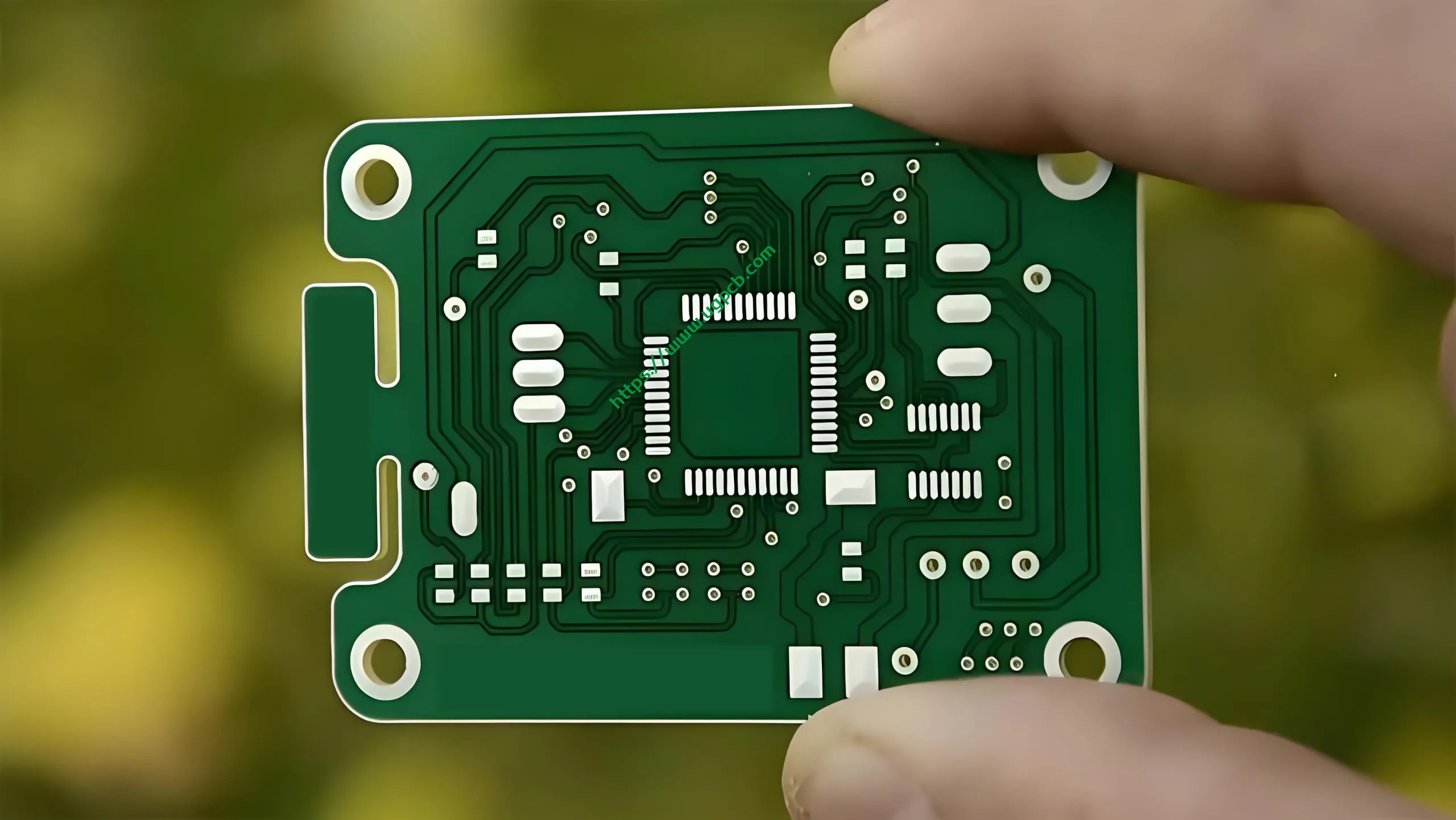
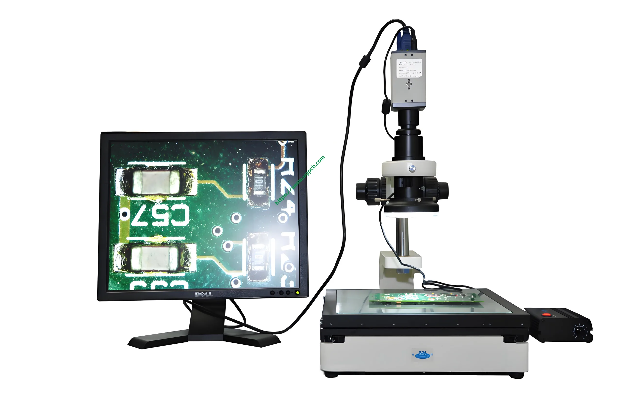
Appearance inspection is the first step in PCB failure analysis. Through visual inspection or using tools such as stereo microscopes and metallographic microscopes, the contamination, corrosion, explosion position, and circuit wiring of PCB are checked. This step aims to quickly locate the failure site and preliminarily determine the failure mode. Par exemple, observe whether the explosion is concentrated in a specific area or whether it is caused by an improper assembly process. Although appearance inspection is simple, it is the basis for subsequent in-depth analysis.
2. X-ray Fluoroscopy: A Fluoroscopic Lens for Internal Defects
For internal defects that cannot be found through appearance inspection, the X-ray fluoroscopy system becomes a powerful assistant. By using the difference in the absorption rate of X-rays by different materials, the X-ray fluoroscopy system can clearly image and inspect the internal defects of PCBA solder joints, internal defects of through-holes, and the quality of solder joints of high-density packaged devices. With the development of technology, industrial X-ray fluoroscopy equipment has micron-level resolution and is moving towards three-dimensional and five-dimensional imaging. Although five-dimensional equipment is expensive, its powerful detection capabilities are impressive.
3. Slice Analysis: A Journey of Exploration of Microstructure
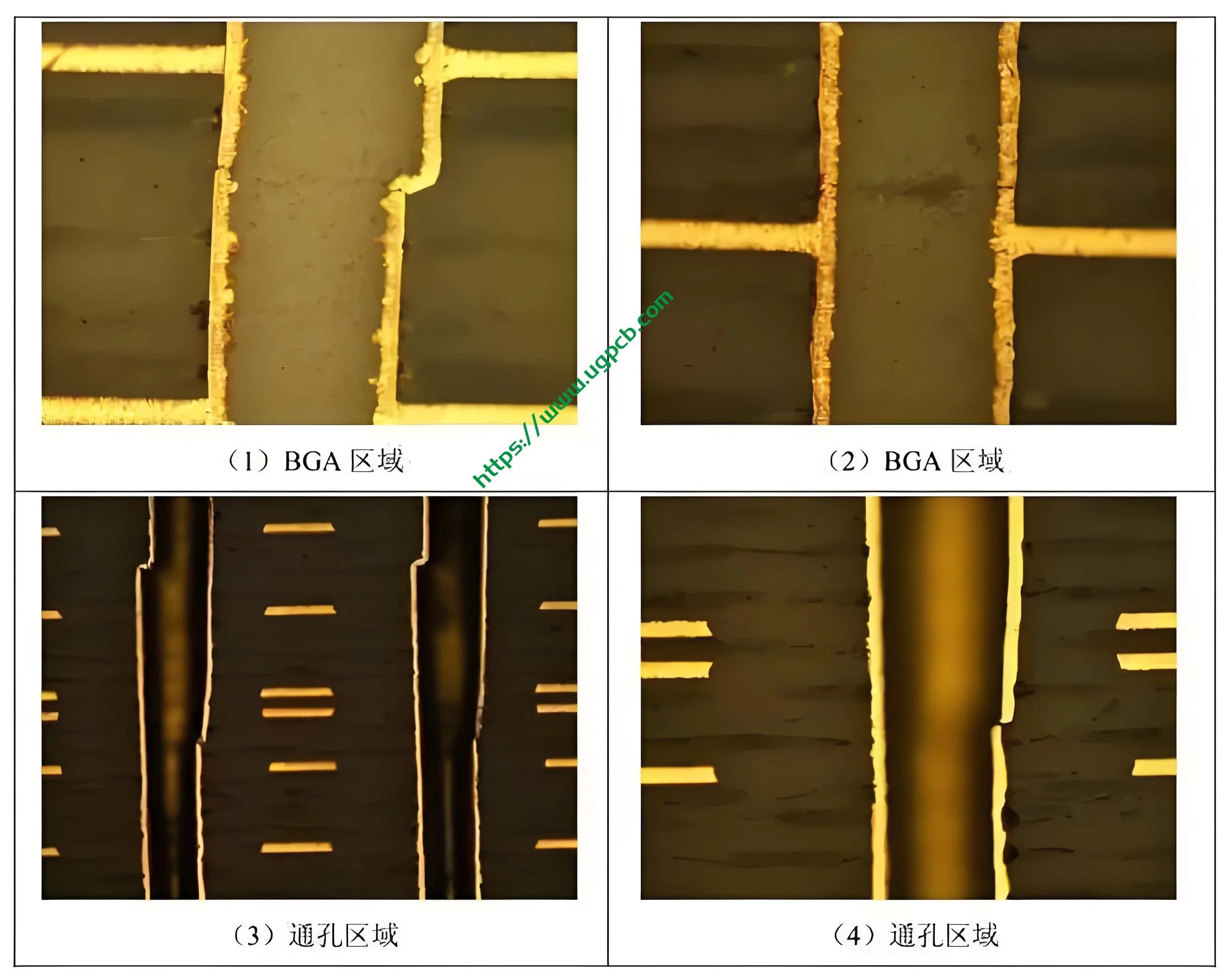
Slice analysis obtains microstructural information of PCB cross-sections through a series of complex steps. Although this method is destructive, it can reveal the microscopic quality of key parts such as through-holes and plating, providing a valuable basis for quality improvement. Slice analysis has high technical requirements and must be strictly implemented in accordance with IPC standards.
4. Scanning Acoustic Microscope: A Powerful Tool for Non-Destructive Testing
Scanning acoustic microscope uses the principle of high-frequency ultrasonic waves reflecting at the material interface to detect defects in components, matériels, and PCBs. Its image marks defects with a red warning color, which is particularly suitable for detecting problems such as explosion and delamination of multi-layer high-density PCBs. Under the lead-free process, the advantages of scanning acoustic microscope are particularly prominent, which can effectively detect the internal delamination and cracking of hygroscopic plastic-sealed devices or substrates.
5. Microscopic Infrared Analysis: Detective of Organic Pollutants
Microscopic infrared analysis combines infrared spectroscopy with microscopy and uses the difference in the absorption of infrared spectra by different materials to analyze the compound composition of the material. This technology is mainly used to detect organic pollutants on the surface of pads or solder joints and analyze the causes of corrosion or poor solderability. Microscopic infrared analysis provides an effective means for the detection of trace pollutants.
6. Scanning Electron Microscope Analysis: An Insight into Fine Structures

Scanning electron microscope (LEQUEL) is an important tool for failure analysis, which can magnify hundreds of thousands of times to observe the surface morphology, metallographic structure, and chemical composition distribution of samples. In PCB analysis, SEM is often used to observe the surface morphology of pads, intermetallic compounds of solder joints, and tin whiskers, etc., to provide intuitive evidence for the analysis of failure mechanisms. SEM images have a large depth of field and are suitable for analyzing uneven samples, such as metallographic structure, microscopic fracture, etc..
7. X-ray Energy Spectrum Analysis: The Revealer of Element Distribution
The X-ray energy spectrometer matched with SEM can analyze the element composition and distribution of the sample surface. Through point analysis, line analysis, and surface analysis, the energy spectrometer can obtain different distribution information of elements, providing strong support for the analysis of the surface composition of the pad and the exploration of the causes of poor solderability.
8. Qualitative and Quantitative Element Analysis
Photoelectron spectroscopy measures the binding energy of the inner shell electrons of atoms to perform qualitative and quantitative element analysis. XPS is particularly suitable for element analysis of the shallow surface (several nanometers) of the sample surface, and can also provide information on the chemical valence state of the elements.
Application in PCB Analysis
In PCB analysis, XPS is mainly used to analyze the quality of pad coating, contaminants, and oxidation degree, revealing the deep-seated causes of poor solderability.
9. Thermal Analysis Differential Scanning Calorimetry (DSC)
Insight into Thermal PropertiesMeasurement of Physical, Chemical, and Thermodynamic Properties
DSC studies the physical, chimique, and thermodynamic properties of materials by measuring the power difference and temperature relationship between a substance and a reference substance.
Application in PCB Analysis
In PCB analysis, DSC is mainly used to measure the degree of curing and glass transition temperature of polymer materials. These two parameters are crucial to the reliability of subsequent PCB processes.
10. Thermomechanical Analyzer (Tma): Test Bench for Deformation Performance
Measurement of Deformation Performance
TMA is used to measure the deformation performance of solids, liquides, and gels under heat or mechanical force.
Application in PCB Analysis
In PCB analysis, TMA is mainly used to measure the linear expansion coefficient and glass transition temperature of PCB. A substrate with an excessively large expansion coefficient may cause the metallized hole to break and fail after welding and assembly. Donc, TMA analysis is of great significance to ensure the reliability of PCB.
Conclusion
With the escort of science and technology, the quality of PCB has been steadily improved. With the development of electronic products towards high density and high performance, and the introduction of environmental protection requirements such as lead-free and halogen-free, the problem of PCB failure has become increasingly complex. By comprehensively applying the above-mentioned failure analysis techniques, we can deeply explore the mechanism and cause of PCB failure, provide a scientific basis for quality control, and thus avoid the recurrence of similar problems. These technologies are like invisible guardians of electronic products, silently guarding the quality and reliability of electronic products, and promoting the development and progress of the electronics industry.
 LOGO UGPCB


