In today’s rapidly developing high-tech, circuits intégrés (ICS) are the cornerstone of information technology, and every step of their manufacturing process embodies the crystallization of human wisdom and technology. Dans ce processus de fabrication complexe et sophistiqué, the Photomask, un élément apparemment ordinaire mais crucial, joue un rôle irremplaçable. Il ne s'agit pas seulement d'un pont reliant la conception de la puce et la fabrication réelle, but also a key factor in determining chip performance and yield. This article will take you to an in-depth understanding of the basic structure and manufacturing process of the Photomask, as well as its role in photolithography, the challenges and optimization measures it faces, and together with all of you, unveil the mystery of the Photomask, le “precision projector”.
The basic structure of the Photomask: the precise combination of quartz and chromium

The Photomask, also known as the Photomask plate, is the core component in the manufacturing process of integrated circuits. It is like a special “template” that accurately transfers the designed circuit pattern to the surface of the wafer. The basic structure of the Photomask consists of two parts: a highly transparent quartz substrate and a chromium shading material with high stability. The quartz substrate, with its high transparency and low thermal expansion coefficient, ensures the penetration of the light source and the stability of the shape; while the chromium layer, as a light-shielding pattern, achieves accurate projection of the circuit design through precise graphical processing. This structure can be figuratively likened to a “printing plate” in printing. Quartz is a high-quality transparent base paper, and the chromium pattern is the designed text or pattern, which works together to project the pattern onto the “printing paper” (wafer).
Photomask manufacturing process: precision engraving from coating to inspection

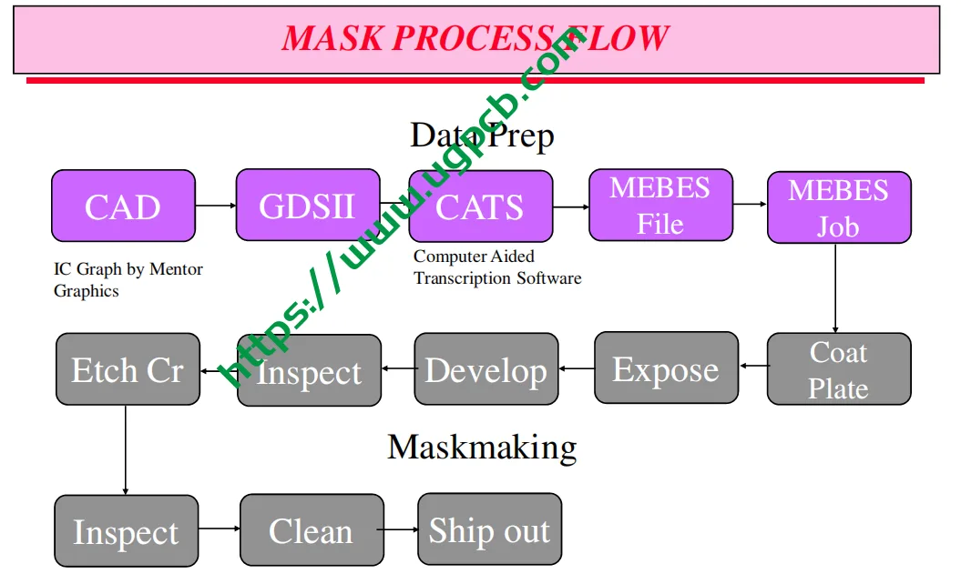
The manufacturing process of the photomask is like a precise “engraving” art. D'abord, a uniform chromium film is deposited on the quartz substrate as a light-shielding layer through physical vapor deposition (PVD) technologie. Ensuite, a layer of photosensitive glue is applied. This layer of glue is sensitive to electron beams and is the key to subsequent graphical processing. Suivant, the photomask is accurately exposed using an electron beam exposure machine. The electron beam is like a carving knife, writing the designed circuit pattern on the photosensitive glue. After exposure, the part of the chromium layer that is not irradiated by the electron beam is retained through steps such as development and etching to form the final circuit pattern. Enfin, after strict cleaning and inspection, ensure that the size, shape and alignment accuracy of the pattern meet the requirements. This process requires not only extremely high precision and stability, but also rich process experience and long-term technical accumulation.
The role of the Photomask in lithography: precise mapping under the projection template

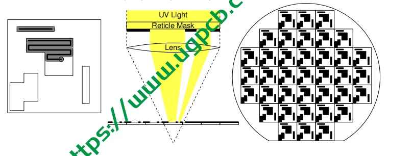
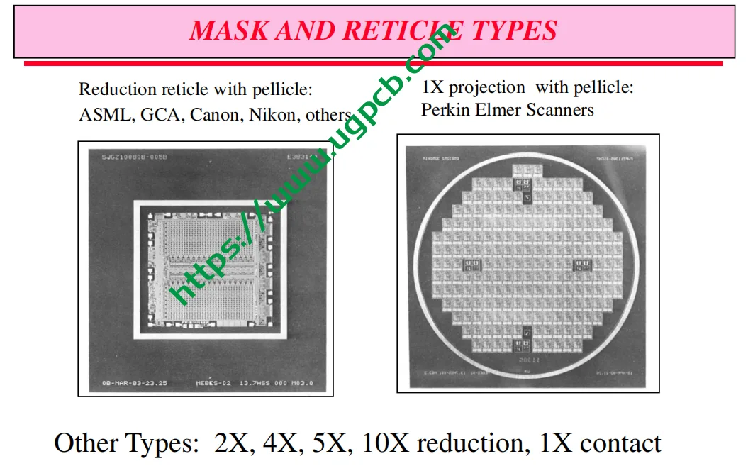
In the lithography process, the Photomask plays the role of a “projection template”. It uses the light source of the lithography machine to project the designed circuit pattern onto the surface of the wafer coated with photoresist. In this process, the light source accurately maps the pattern onto the wafer through the transparent area of the Photomask. Since the pattern on the Photomask is generally 4 times the size of the circuit design drawing, it is reduced to 1/4 by the projection system of the lithography machine and then projected onto the wafer. This reduction not only improves the resolution, but also reduces the manufacturing error. This role of the Photomask can be figuratively likened to the “slide” of the projector. Through the projection of light, the pattern is mapped onto the screen (wafer), realizing the precise conversion from design to manufacturing.
Challenges and optimization of Photomask technology: a road of continuous breakthroughs in innovation
With the continuous advancement of chip manufacturing, Photomask manufacturing and use are facing more and more challenges. In order to meet the needs of high-precision lithography, people have introduced a variety of advanced optimization measures. Optical proximity correction (OPC) technology compensates for the shape deviation caused by the diffraction effect of light by accurately adjusting the Photomask pattern; phase shift Photomask (PSM) enhances the contrast of the pattern and improves the resolution by introducing phase difference; the particularity of EUV Photomaskmask requires the use of multilayer films and more complex reflective structures to adapt to the high energy of extreme ultraviolet light; and in terms of dust prevention and protection, the application of Pellicle is like the film on the mobile phone screen, which protects the Photomask without affecting the exposure effect. The application of these innovative technologies continues to push the boundaries of Photomask technology and provides more accurate and reliable guarantees for chip manufacturing.
The significance of Photomask manufacturing to the industry: the only way to self-control
The manufacturing of Photomasks is an indispensable part of the integrated circuit industry chain. Its complexity and precision requirements are extremely high, which is directly related to the success or failure of chip production. Cependant, at present, the global high-end Photomask manufacturing equipment and materials are heavily dependent on a few countries and enterprises, and China still has obvious shortcomings in this field. Technical barriers in equipment, matériels, experience accumulation, etc.. make the breakthrough of domestic Photomask the key to improving China’s independent chip manufacturing capabilities. Donc, whether it is from the aspects of Photomask materials, équipement, or process technology, a lot of resources need to be invested in research and development to achieve the construction of an independent and controllable industrial chain.
Conclusion: Masque photo – la précision “projecteur” of chip manufacturing
As the core component in the integrated circuit manufacturing process, the precision and quality of the Photomask directly determine the performance and yield of the chip. From the basic structure to the manufacturing process, from the role of lithography to technical challenges and optimization, every step of the Photomask embodies the power of science and technology and human wisdom. With the continuous advancement of advanced process nodes, the technical threshold and complexity of the Photomask continue to increase, posing new challenges to materials, équipement, and processes. Cependant, it is these challenges that drive the continuous innovation and development of Photomask technology, providing more accurate and reliable guarantees for chip manufacturing. À l'avenir, with the continuous breakthrough and improvement of domestic technology, China’s chip manufacturing industry will usher in a broader development prospect. The Photomask, la précision “projecteur” of chip manufacturing, will continue to shine on the high-tech stage.
 LOGO UGPCB

