Dans le vaste univers de l'industrie électronique, l'importance des circuits imprimés (PCB) car les ponts reliant les composants électroniques vont de soi. Cependant, avec le développement rapide de la science et de la technologie, traditional PCBs seem to be unable to cope with the packaging of high-power devices. In order to break through this bottleneck, a series of innovative technologies have emerged, among which the technology of embedding power devices in PCBs is the most dazzling star. This article will take you into the mysterious world of this technology and explore its principles, current status and future trends.
1.Limitations and challenges of traditional PCBs
PCB, le “electronic highway” composed of organic insulation layer and metal circuit layer, has become an indispensable component in electronic products with its low price and good machinability. Cependant, just as everything has its limitations, the inadequacy of traditional PCBs in heat dissipation performance has become a major bottleneck restricting its application in the field of high-power device packaging.
The organic insulation layer, usually made of organic resin material and glass fiber cloth (FR4), has a thermal conductivity of only 0.2~0.3W/(m·K), which is much lower than the thermal conductivity of metal materials. In high temperature environment, organic materials are prone to thermal degradation and thermal aging, and even carbonization may occur in severe cases, which seriously affects the stability and life of electronic products. Donc, it is difficult for traditional PCBs to meet the high requirements of power device packaging for heat dissipation performance.
2.The emergence of metal-based printed circuit boards (MCPCBs)

In order to improve the heat dissipation performance of PCB substrates, metal-based printed circuit boards (MCPCBs) came into being. MCPCBs combine metal layers and insulating layers, and use the high thermal conductivity of metal to improve the overall heat dissipation capacity of the substrate. Cependant, although MCPCBs have improved in heat dissipation performance, their overall thermal conductivity is still not high, which makes it difficult to meet the ultimate pursuit of heat dissipation performance for high-power device packaging.
3.Breakthroughs in buried copper plate technology

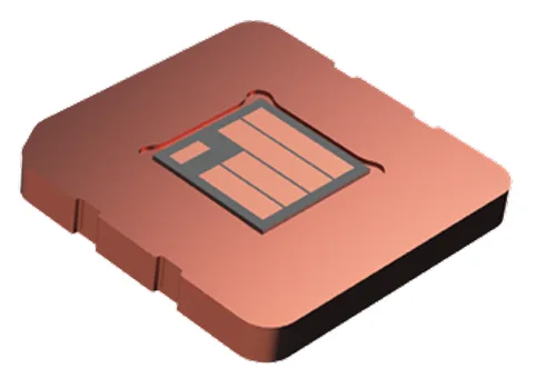
In order to further improve the heat dissipation performance of PCB substrates, the industry has proposed the concept of buried copper plates. The buried copper plate technology uses a lamination process to embed metal copper blocks into windowed PCB or MCPCB substrates, and uses the high thermal conductivity of metal to significantly improve the overall heat dissipation capacity of the substrate. Cependant, in order to avoid short circuits caused by metal conduction, the surface of the copper block usually needs to be covered with an insulating layer. Although this insulating layer solves the short circuit problem, it also has a certain impact on the heat dissipation performance of the substrate.
4.Jinmai: Innovative practice of embedding standard power devices into packaged PCB

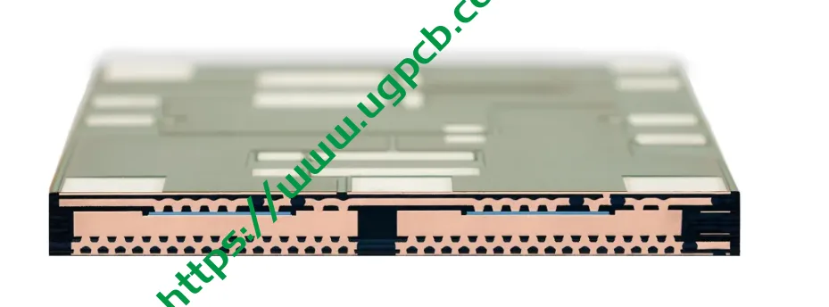
Against this background, Jinmai (a subsidiary of Infineon Technologies, which is the agent of Inheng) applied for a utility model patent for “embedded packaged PCB for standard power devices” (application number: CN202323630195.1). The patent proposes a new packaging structure that integrates power chips, control circuits and drive circuits, busbars and shunt resistors into a PCB, achieving high integration and modularization.
Spécifiquement, the PCB structure of the patent includes six packaging layers, wherein a carrier unit is provided between the third packaging layer and the fourth packaging layer. The carrier unit includes a copper substrate, the upper surface of which is provided with a groove, and the inner bottom of the groove is fixedly connected to the power chip through a connecting layer. This structure not only expands the heat conduction area, but also minimizes the impact of the insulation layer on the heat dissipation performance by optimizing the layout and thickness of the insulation layer.

It is worth noting that Jinmai’s integration solution is likely to be designed based on Infineon’s S-cell chip. As Infineon’s star product, the S-cell chip has won wide recognition in the market for its excellent performance and stability. Jinmai applied it to its own packaging solution, which undoubtedly further enhanced the competitiveness of the product.
Cependant, there are also some issues worth exploring in this solution. Par exemple, the power device is isolated from the mounting heat-conducting surface by an insulating layer, and the thickness and thermal conductivity of this layer have a greater impact on the thermal resistance. Although there is a large copper base to expand the heat-conducting area, the existence of the insulating layer will still have certain limitations on the heat dissipation performance. En outre, whether the embedded shunt resistor is suitable for high-power applications is also worth discussing. Large current loss is large, the resistance value is very small, and whether the temperature drift will affect the accuracy and other issues need further research and verification.
5.Shenzhen South Circuit: Innovative Exploration of Embedded Power Chip Packaging Substrate and Packaging Method
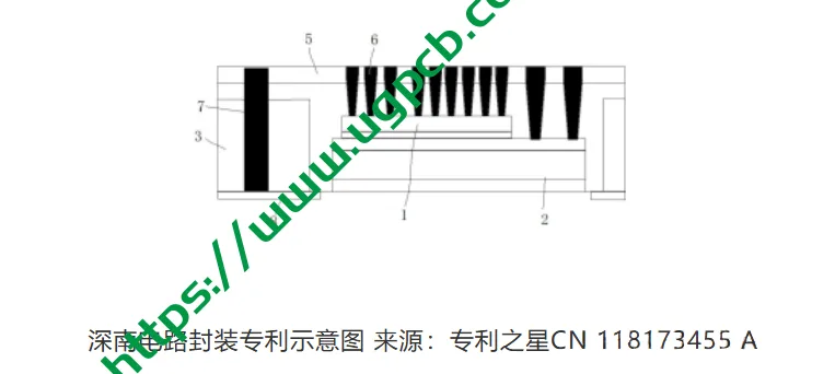
In addition to Jinmai, Shenzhen South Circuit has also conducted in-depth exploration in the field of power device embedded PCB technology. They proposed a power chip embedded packaging substrate and packaging method, which realizes efficient packaging and heat dissipation of power chips through bare chips, rigid substrates, core boards, insulating layers, external metal layers, blind holes on the metal layer surface, connecting columns and internal metal layers.

This solution not only improves the packaging density and heat dissipation performance, but also reduces the packaging cost and manufacturing difficulty by optimizing the internal structure. This innovative practice of Shenzhen South Circuit provides new ideas and directions for the development of power device embedded PCB technology.
6.Future Outlook: Infinite Possibilities of Power Device Embedded PCB Technology
With the continuous development of the electronics industry, power device embedded PCB technology will usher in a broader development prospect. D'une part, with the continuous emergence of new materials and new processes, the heat dissipation performance of PCB substrates will be further improved; on the other hand, with the rapid development of intelligent manufacturing and Internet of Things technology, power device embedded PCB technology will be widely used in smart homes, new energy vehicles, industrial automation and other fields, providing strong support for innovation and development in these fields.
À l'avenir, we have reason to believe that power device embedded PCB technology will continue to break through technical bottlenecks and achieve more efficient, reliable and intelligent packaging and heat dissipation solutions. This technological innovation will lead us to a better electronic world.
________________________________________
 LOGO UGPCB

