In today’s rapidly evolving electronic product landscape, miniaturization and high performance have become irreversible trends. With the widespread adoption of smartphones, wearable devices, and various smart IoT products, cartes de circuits imprimés (PCB), as the neural center of electronic devices, are facing increasing design complexity and integration levels. Against this backdrop, VIPPO (Capping/POVF) technology is emerging as a key link in high-density PCB manufacturing, particularly in applications on BGA (Tableau de grille à billes) coussinets, showcasing unparalleled advantages.
Traditional Challenges and the Birth of VIPPO

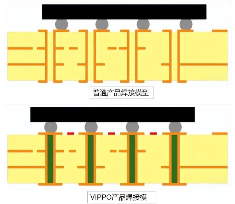
A comparison diagram of soldering models between ordinary PCB and VIPPO technology PCB.

VIPPO
In traditional PCB design, through-holes were primarily used for electrical connections between components. Cependant, with the dramatic increase in wiring density, traditional through-holes struggle to meet the demands of high-density routing. The advent of microvia technology alleviated this issue to some extent by enabling higher density circuit connections through smaller hole sizes and tighter arrangements. Yet, reliability concerns limited its application in some high-end products. Par conséquent, there was an urgent need in the industry for a novel via treatm
ent technology that could satisfy both high-density connection requirements and ensure reliability, leading to the development of VIPPO technology.

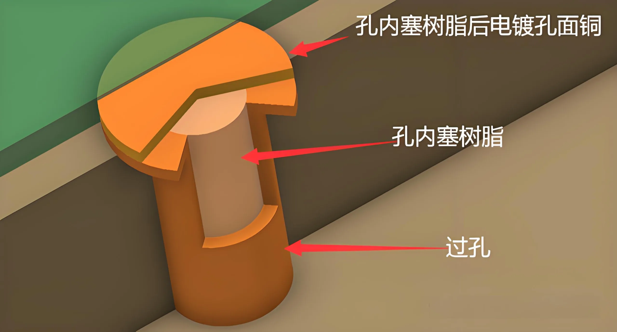
VIPPO Structure Diagram
VIPPO technology, short for Via In Pad with Plated Overfill, innovates by filling conductive material inside the via and adding a layer of copper cap flush with the pad surface at the via entrance. This design not only solves solderability issues but also effectively prevents the ingress of solder paste or flux during the SMT (Technologie de montage de surface) processus, avoiding risks associated with gas production affecting soldering quality.
Manufacturing Process and Technological Innovation
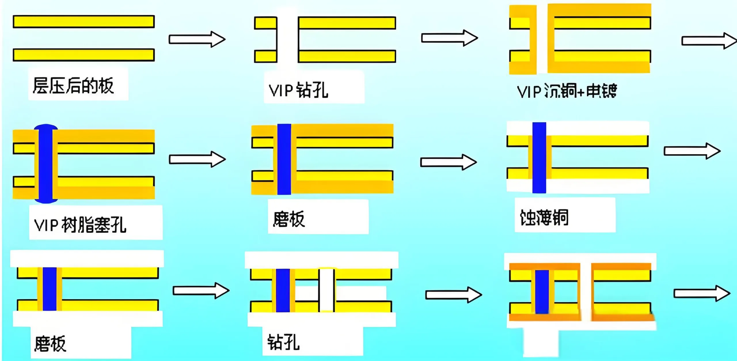
The manufacturing process of VIPPO technology mainly involves drilling, via plugging, and copper cap addition. Compared to traditional full or half plugging processes, VIPPO’s unique feature lies in its copper cap design, significantly enhancing PCB soldering performance and reliability. Cependant, adopting this technology also leads to increased manufacturing costs, estimated to rise by approximately 15% à 25%. De plus, due to the bonding strength between the copper cap and the pad, there’s a risk of pad detachment during the soldering process, necessitating more precise process control from manufacturers.

VIPPO Process
To address the weak bonding force between resin and copper, the industry has gradually standardized VIPPO technology processes, introducing two major innovations: premièrement, by reducing the base copper thickness through etching and increasing the thickness of secondary electroplating (Capping copper) to ensure a finished copper cap thickness of at least 15 micromètres, thereby enhancing bonding force and conductivity; deuxièmement, using a chemical copper process to make the via surface resin plateable, further improving the bonding force between the copper cap and resin and ensuring stability during soldering.
Diverse Applications of VIPPO Technology
Beyond high-density connections on BGA pads, VIPPO technology also stands out in HDI (Interconnexion à haute densité) technology via stacking applications. By adopting VIPPO technology, it’s possible to reduce the number of pressing and laser drilling operations, transitioning from arbitrary interconnection structures to standard two-layer HDI designs. This not only lowers production costs but also shortens lead times (LT), supporting rapid iteration of electronic products.
En plus, VIPPO technology effectively eliminates capacitive effects. In conventional BO/BO (Buried and Blind Via) structures, ground layers beneath often cause capacitive effects that degrade signal transmission quality. Applying VIPPO technology modifies the via structure to reduce these capacitive effects, enhancing overall board performance.
Key Control Points and IPC Standards
Strict quality control is crucial during the implementation of VIPPO technology. The IPC-6012 standard specifies clear requirements for critical parameters of VIPPO technology, including Capping copper thickness, Wrap thickness, and Wrap length. Accurate control of these parameters directly impacts PCB electrical performance and reliability.

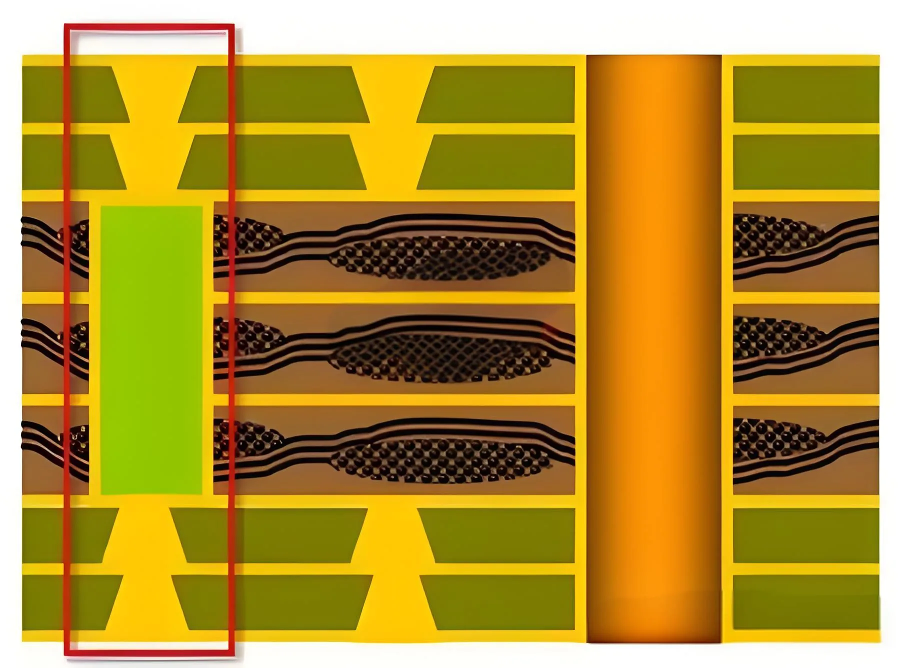
VIPPO slice
(Note: The diagram above is a schematic cross-sectional view; actual VIPPO technology cross-sections should be inspected in detail according to the IPC-6012 standard.)
By examining the cross-sectional diagram against IPC standards, one can verify whether parameters meet requirements, such as if the Capping copper thickness reaches the minimum specified value and if the Wrap thickness and length are uniform. These checks are vital for ensuring the quality of VIPPO technology.
Conclusion
As an innovative achievement in the PCB industry, VIPPO technology not only resolves technical challenges in high-density connections but also supports the miniaturization and high performance of electronic products. With ongoing technological maturation and cost optimization, VIPPO technology is poised for broader applications, propelling electronic manufacturing to new heights. À l'avenir, as technologies like 5G and IoT deepen, VIPPO technology will play an even more significant role, becoming a bridge and bond connecting the digital world.
 LOGO UGPCB

