
PCB HDI
UGPCB HDI PCB Solutions: Redefining High-Density Electronic Design Limits with Microvia Interconnect Technology
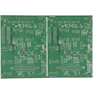
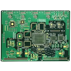
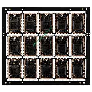
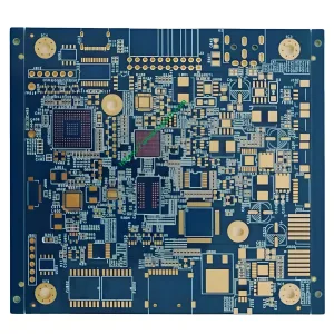
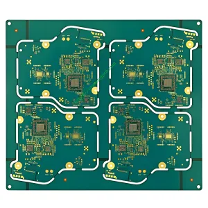
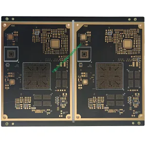
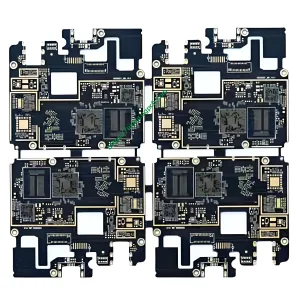
In the era of continuous miniaturization of smartphones, appareils portables, and advanced medical instruments, UGPCB leverages over a decade of HDI PCB R&D expertise to showcase cutting-edge capabilities in its corporate website’s “PCB HDI” section. From 1-step to Any-layer high-density interconnect boards, we break through traditional PCB design bottlenecks via laser drilling, precision circuitry, and stack-up optimization, empowering clients to achieve 50% higher component density and doubled signal transmission speeds.
Core Technical Advantages: Redefining HDI PCB Performance Standards
Ultra-High-Density Interconnect Architecture
- Any-Layer Interconnect Technology: Mass-produce Any-layer HDI boards with 0.05mm laser microvias (full L1-L10 penetration), 40/40μm trace width/spacing, and 3x increased routing density.
- Hybrid Stack-Up Design: Integrate FR-4, MEGTRON®7, and Rogers materials to ensure Dk value stability (±0.02) et 25% lower insertion loss compared to conventional HDI solutions.
Precision Manufacturing Process System
- Laser Drilling Accuracy: CO₂/UV laser hybrid processes achieve ±10μm hole diameter tolerance and ≤0.8μm hole wall roughness, ensuring high-frequency signal integrity.
- Ultra-Thin Dielectric Layer Control: Dynamic prepreg lamination technology guarantees ±5% dielectric thickness uniformity and Z-axis expansion rate <3% pour 20+ layer HDI boards.
Signal Integrity and Reliability Assurance
- Cross-Layer Impedance Control: Cadence Sigrity simulations enable ±6% impedance tolerance for 56Gbps PAM4 signals and >40dB@10GHz crosstalk suppression.
- Thermal Stress Management: Copper pillar filling combined with low-CTE substrates (par ex., TUC TU-862HF) passes 3,000 thermal cycles (-40℃↔125℃) with zero microcracks.
Typical Applications and Technical Benchmarks
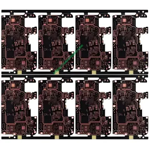
- 5G Smartphone Motherboards: 10-layer Any-layer HDI with 0.3mm thickness and 0.25mm pitch BGA integration, supporting mmWave antenna module mass production.
- High-End Medical Endoscopes: 6-step HDI flexible boards with 30/30μm trace width/spacing, enduring >100,000 bends (IPC-6013D Class 3 normes).
- Automotive ADAS Domain Controllers: 16-layer HDI + heavy copper design (4oz inner layers), integrating 77GHz radar and Gigabit Ethernet, certified to AEC-Q100 Grade 2.
End-to-End Service System and Certifications
- Collaborative Design Support: Polar SI 9000 impedance modeling, Mentor Xpedition HDI routing optimization, and Valor NPI manufacturability analysis.
- Prototypage rapide: 5-day delivery for 8-layer HDI boards, 10-day delivery for Any-layer HDI samples, supporting complex blind/buried via stacks (1-2-3-…-n).
- Stringent Quality Control: 100% compliance with IPC-6016 Class 3, OIN 13485 medical electronics certification, and IATF 16949 automotive reliability standards.
Three Key Values of Choosing UGPCB HDI PCBs
- Technology Leadership: 100+ HDI patents, with a technical database covering 0.3mm ultra-thin boards and 56G high-speed signal scenarios.
- Cost Efficiency: Intelligent panelization algorithms improve material utilization by 18%, while hybrid-step designs reduce BOM costs by 25%-40%.
- Mass Production Assurance: Fully automated AOI+AXI inspection systems ensure >99% yield for bulk orders and support million-unit production capacity.
Get Your Custom UGPCB HDI PCB Solution Now
Visit the “PCB HDI” section on our official website, submit your requirements, and receive:
✅ Any-layer stack-up simulation reports
✅ High-speed signal integrity pre-analysis
✅ 24-hour rapid quotation response
 LOGO UGPCB


WeChat
Scannez le code QR avec WeChat