Technical Features
Impedance Specifications
- 50 Ω Antenna
- 90Oh & 100Ω Differential Impedance
Applications
Electronique grand public
- Cell Phones
- Tablets
- Ultrabooks
- E-Readers
- MP3 Players
- GPS
- Portable Game Consoles
- DSCs (Digital Still Cameras)
- Cameras
- LCD TVs
- POS Terminals
Other Applications
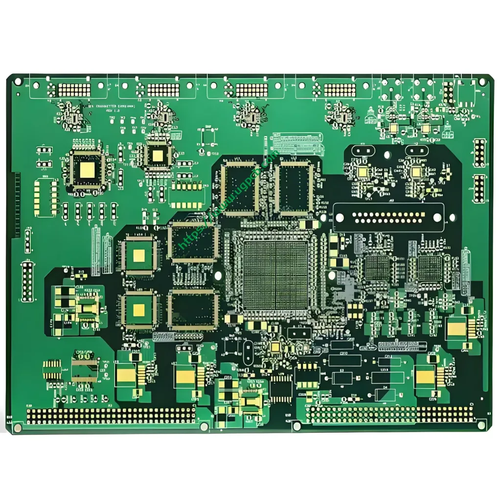
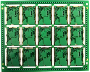
HDI PCBs are widely used to reduce the weight and overall size of products, as well as improve the electrical performance of devices. High-density PCBs are often found in:
- Téléphones portables
- Touch screen devices
- Laptops
- Digital cameras
- 4G network communications
En plus, HDI PCB technology plays a crucial role in:
- Medical equipment
- Various electronic aircraft components
The possibilities for high-density interconnect PCB technology seem almost limitless, offering significant advantages in terms of size, poids, and electrical performance across a wide range of applications.
 LOGO UGPCB

