
Overview of the 14 PCB de bobine de cuivre lourd de couche
Le 14 Layer Heavy Copper Coil PCB is a high-density, multilayer power board designed for applications requiring robust electrical performance and reliability. This PCB is ideal for complex electronic systems that need to manage high power and signal integrity.
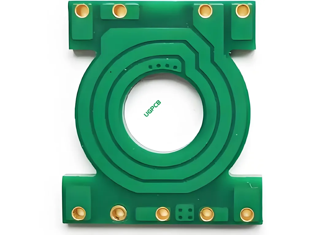
What is a 14 PCB de bobine de cuivre lourd de couche?
UN 14 Layer Heavy Copper Coil PCB is a printed circuit board (PCB) avec 14 layers of copper traces, each weighing 4 ounces per square foot. This type of PCB is specifically designed for power applications, where it needs to handle large currents and provide stable electrical connections.
Exigences de conception
The design requirements for a 14 Layer Heavy Copper Coil PCB are stringent to ensure its performance and reliability:
- Matériel: EM827, chosen for its excellent electrical and thermal properties.
- Nombre de couches: 14 layers to accommodate complex and dense circuit designs.
- Couleur: Green/White for easy identification and aesthetic appeal.
- Épaisseur finie: 4.0mm to provide structural integrity and durability.
- Épaisseur du cuivre: 4OZ to ensure adequate conductivity and heat dissipation.
- Traitement de surface: Immersion Gold to enhance solderability and corrosion resistance.
- Épaisseur de cuivre dans le trou: 70UM for better electrical connectivity.
- Largeur de ligne: 0.3mm to support fine circuit patterns.
- Ouverture minimale: 0.4mm to allow precise component placement.
Comment ça marche?
Le 14 Layer Heavy Copper Coil PCB works by providing a platform for various electronic components to be interconnected through conductive pathways. These pathways, or traces, are made of copper and are etched onto the board. The immersion gold surface treatment ensures that these traces remain conductive and resistant to environmental factors.
Applications
The primary application of the 14 Layer Heavy Copper Coil PCB is in power electronics where it manages and regulates the flow of electrical power. This includes:
- Alimentations
- Motor drives
- Renewable energy systems
- Industrial control systems
Classification
Based on its features and applications, le 14 Layer Heavy Copper Coil PCB can be classified as a high-power PCB designed for demanding power applications. This classification highlights its capability to handle large currents and provide stable electrical connections.
Composition des matériaux
The core material used in the 14 Layer Heavy Copper Coil PCB is EM827, a high-performance laminate material known for its excellent mechanical, thermique, et propriétés électriques. This material ensures that the PCB can withstand the demands of power applications.
Caractéristiques de performance
The performance characteristics of the 14 Layer Heavy Copper Coil PCB include:
- High power handling capacity
- Excellent signal integrity
- Superior thermal management
- Robust mechanical strength
- Long-term stability
Structural Details
The structural details of the 14 Layer Heavy Copper Coil PCB are as follows:
- Nombre de couches: 14 couches
- Épaisseur finie: 4.0mm
- Épaisseur du cuivre: 4once
- Traitement de surface: Immersion Or
- Épaisseur de cuivre dans le trou: 70UN
- Largeur de ligne: 0.3mm
- Ouverture minimale: 0.4mm
Features and Benefits
The key features and benefits of the 14 Layer Heavy Copper Coil PCB include:
- High density interconnectivity
- Excellent power handling capacity
- Robust mechanical construction
- Reliable long-term performance
- Aesthetic color options (Vert/Blanc)
Processus de production
The production process of the 14 Layer Heavy Copper Coil PCB involves several steps, y compris:
- Sélection des matériaux: Choosing high-quality EM827 material.
- Empilement de calques: Arranging the 14 layers with precision.
- Gravure: Removing excess copper to form the desired trace patterns.
- Placage: Applying immersion gold surface treatment.
- Assemblée: Incorporating PTHs and vias for layer interconnections.
- Essai: Ensuring the PCB meets all performance specifications.
Cas d'utilisation
Le 14 Layer Heavy Copper Coil PCB is used in various scenarios such as:
- High-power industrial equipment
- Renewable energy systems
- Motor drive controllers
- Power supply units


