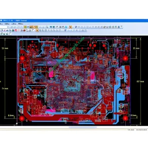
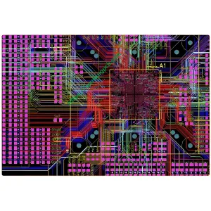
Definition and Structure
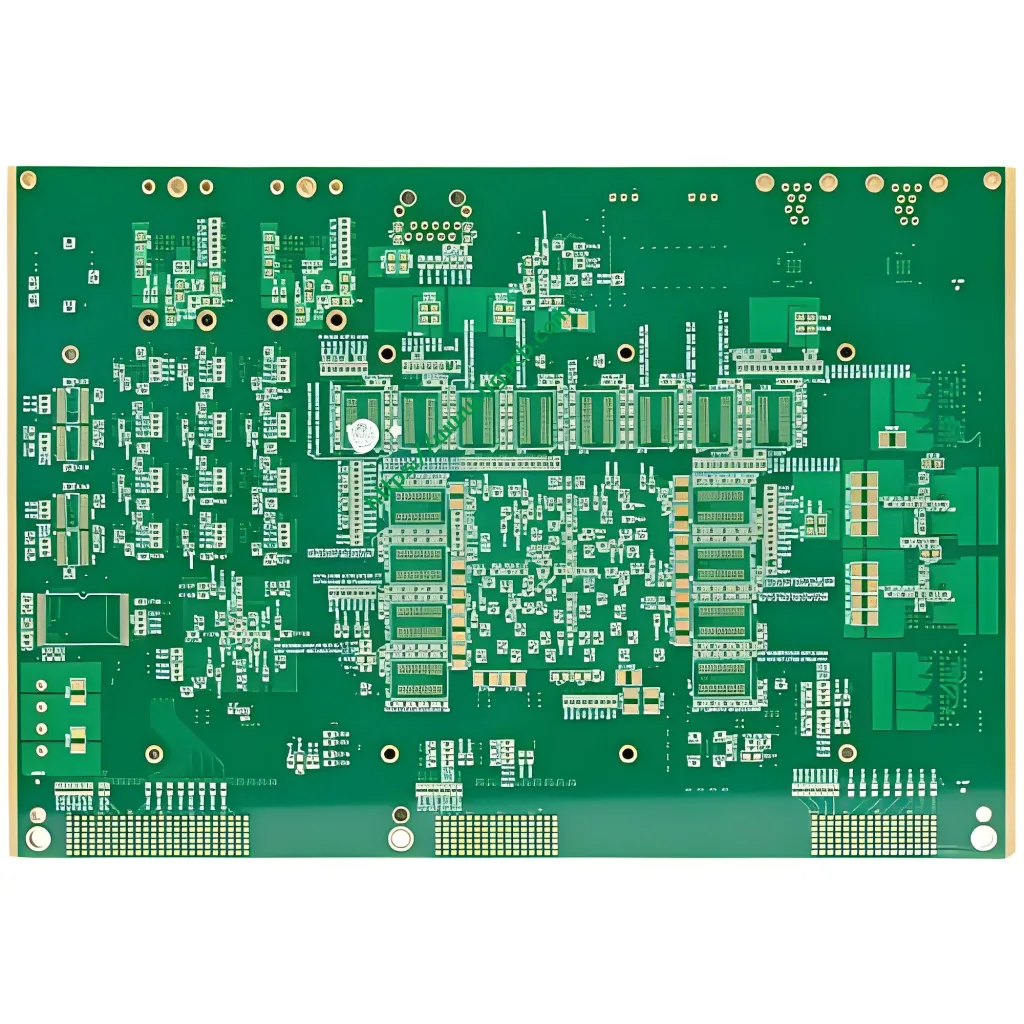
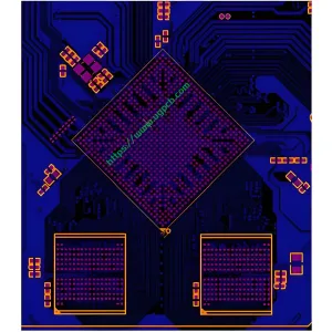
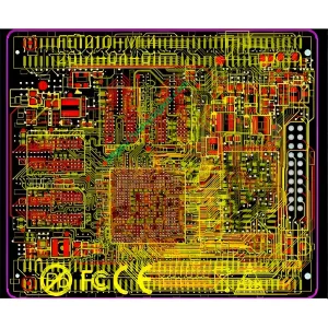
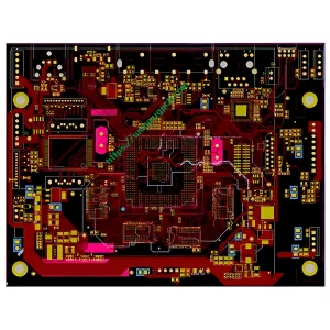
A 24-layer PCB is an advanced multilayer board with 24 copper layers. The PCB includes signal layers, ground planes, and power planes. En outre, this PCB consists of silk screen, solder mask, etc.. A 24-layer PCB is about 5mm thick. It provides dimensional stability due to the high number of layers in it.
Compatibility and Material Properties
The manufacturer effectively arranges the ground and signal layers. This helps ensure that the PCB is compatible with HDI applications. These applications are high density interconnects. The materials used in the 24-layer PCB ensure a low dielectric constant. En plus, the dielectric materials used in this advanced multilayer board are thin. So this helps to create tight coupling between layers.
Materials for 24-layer PCBs
Base Materials
A 24-layer PCB contains different materials in its manufacture. It uses materials such as copper foil, FR4, CEM3, and epoxy resin. In this PCB, the manufacturer presses and bonds the copper foil and fiberglass resin material together. FR4 is a PCB material that provides sufficient rigidity in electronics. It provides sufficient glass transition temperature.
Additional Properties
En outre, the material has excellent moisture resistance. This means that PCBs containing FR4 can withstand high temperatures. En outre, this material allows for a suitable dielectric strength. Silkscreen, FR4, and solder mask are the base materials for a 24-layer PCB. High transition glass temperature is an important feature of 24-layer PCBs.
Other Materials
Other materials used for 24-layer PCB fabrication include copper foils and prepregs. 24-layer PCBs can have different copper thicknesses. The thickness and number of layers of copper help it conduct high current loads.
What is a 24-layer PCB stackup?
Definition and Importance
A 24-layer PCB stackup is an arrangement of the upper layers on a circuit board. In a multilayer PCB, there are several ways to place copper layers on the board. Manufacturers consider a few important factors before arranging for a multi-layer stack.
Components of the Stackup
In a 24-layer stack, there are routing layers, ground planes, and power planes. The wiring layer can be the top layer, middle layer, or bottom layer. Ground and power planes are very important in this stackup. The routing layer creates interconnections between components. Manufacturers can place routing layers on the bottom, haut, or middle layers. It depends on the application requirements of the board. Signal routing is a critical part of multilayer boards. The stack-up configuration of a 24-layer PCB determines its functionality. A well-aligned stackup will ensure signal routing in the PCB.
24-Couper la fabrication de PCB
Manufacturing Processes
The manufacture of a 24-layer PCB involves certain processes. Since such a PCB has ten layers of conductive material, its fabrication is complicated. Manufacturers laminate core and prepreg layers under high pressure and high temperature.
Lamination and Adhesive Processes
Durant ce processus, the manufacturer ensures that there is no air between the PCB layers. They also ensure that the adhesive that holds the layer melts properly. A 24-layer PCB consists of a variety of materials. Core and prepreg are similar materials. Cependant, prepregs are more ductile than core materials. This is because it is not fully cured. When the manufacturer applies high temperatures to the layup, the prepreg melts. The layers are then connected together. After cooling, the result is a solid 24-layer board. Manufacturers apply solder masks to multilayer boards. The role of the solder mask is to prevent short circuits in the traces.
Detailed Manufacturing Steps
The inner layer of the multilayer board includes a core of fiberglass and epoxy resin. Prepreg laminates these layers together. The manufacturer stacks the inner layers together to ensure the layers are aligned.
The manufacturing process of a 24-layer PCB is outlined as follows:
- Inner layer imaging and etching
- Inner layer lamination
- Drilled plate
- Outer layer imaging
- Plating and etching
- Outer layer etch stripping
- Solder mask
- Screen printing
- Test
Advantages of 24-layer PCB
Enhanced Functionality
This PCB helps to enhance the functionality of electronic devices. The 24-layer board has the huge advantage that the project needs. Some of these advantages are:
Conception compacte
24-layer PCB supports compact design. The PCB has ground and signal layers placed on each other. This board is ideal for small devices like laptops, cell phones, etc.. Electronic devices are getting smaller and more complex. 24-layer PCBs are ideal for complex and tiny devices.
Temperature Resistance
The 24-layer PCB can work at different temperatures. This PCB is designed to work at different temperatures. 24-layer boards are ideal for high-performance and high-end applications.
High Current Conduction
Another important advantage of this type of PCB is the ability to carry high current loads. The PCB has different copper thicknesses. It can withstand high power.
High Functionality
A 24-layer PCB is very practical. Donc, it is widely used in high-density interconnect and high-power projects. En outre, the PCB increases the efficiency of high-speed projects.
 LOGO UGPCB
