
Overview of 4layers Multilayer Bluetooth PCB
The 4-layer multilayer Bluetooth PCB is a specialized product designed to meet the stringent requirements of Bluetooth applications. This type of PCB offers high signal integrity, stabilité thermique, et fiabilité, making it an ideal choice for various Bluetooth-enabled devices.
Définition
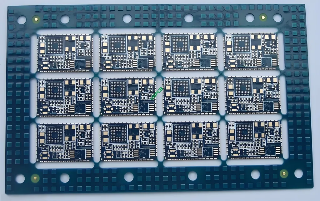
A 4-layer multilayer Bluetooth PCB is a printed circuit board specifically designed to support the functions of a Bluetooth module. Il se compose de plusieurs couches de matériaux conducteurs et isolants, providing complex electrical pathways and connections essential for the operation of the Bluetooth device. Le terme “4-couche” refers to the number of conductive layers, while “multilayer” indicates that it has more than two layers of conductive material.
Exigences de conception
When designing a 4-layer multilayer Bluetooth PCB, Plusieurs exigences clés doivent être satisfaites:
- Material Quality: High-quality FR4 material is essential for durability and thermal stability.
- Layer Configuration: A 2-layer design is standard, allowing for efficient routing of signals and power.
- Épaisseur du cuivre: A copper thickness of 1OZ ensures adequate conductivity.
- Traitement de surface: Immersion gold surface treatment enhances connectivity and corrosion resistance.
- Trace/Space Dimensions: Minimum trace and space dimensions of 4mil (0.1mm) are required for precise circuit patterns.
- Special Features: Half-hole PCB design is often incorporated for specific component placement and soldering requirements.
Principe de fonctionnement
The 4-layer multilayer Bluetooth PCB operates based on the principles of electrical conductivity and signal integrity. Conductive layers form the pathways for electrical signals, while insulating layers prevent unwanted interactions between these signals. The half-hole design allows for better signal routing and reduces crosstalk. Le traitement de surface d'or à l'immersion offre une excellente connectivité et protège contre les facteurs environnementaux.
Applications
This type of PCB is primarily used in Bluetooth-enabled devices, which are crucial components in various electronic systems such as wireless communication devices, audio equipment, and IoT (Internet des objets) devices. Ceux-ci incluent:
- Bluetooth speakers and headphones
- Wireless keyboards and mice
- Smart home devices
- Fitness trackers and wearables
- Industrial automation systems
Classification
4-layer multilayer Bluetooth PCBs can be classified based on their specific features and intended use, tel que:
- Signal Integrity Boards: For maintaining high signal quality in Bluetooth communications.
- Thermal Management Boards: To efficiently dissipate heat generated by Bluetooth components.
- Tableaux de contrôle: For managing and controlling various functions in Bluetooth-enabled systems.
Matériels
The primary materials used in the construction of a 4-layer multilayer Bluetooth PCB include:
- Matériau de base: FR4, a flame-retardant fiberglass material known for its excellent dielectric properties and mechanical strength.
- Conductive Material: Cuivre, used for the conductive traces.
- Traitement de surface: L'or d'immersion, which enhances connectivity and provides corrosion resistance.
Performance
The performance of a 4-layer multilayer Bluetooth PCB is characterized by:
- High Signal Integrity: Due to the precise trace and space dimensions and half-hole design.
- Enhanced Thermal Stability: The FR4 base material helps dissipate heat more effectively.
- Reliable Connectivity: Ensured by the immersion gold surface treatment.
- Durability: Enhanced by the robust FR4 base material.
- Electrical Efficiency: Minimized signal loss and interference due to optimized layer configuration.
Structure
The structure of a 4-layer multilayer Bluetooth PCB consists of:
- Two Layers of Conductive Material: Alternating with insulating layers.
- Immersion Gold Surface Treatment: For enhanced connectivity and protection.
- Half-Hole Design: For specific component placement and soldering requirements.
Caractéristiques
Key features of the 4-layer multilayer Bluetooth PCB include:
- Advanced Layer Configuration: 4-layer design for superior signal routing.
- High Precision: With minimum trace and space dimensions of 4mil (0.1mm).
- Customizable Color Options: Available in black or white.
- Standard Thickness: Avec une épaisseur finie de 1,0 mm.
Processus de production
The production process for a 4-layer multilayer Bluetooth PCB involves several steps:
- Préparation des matériaux: Selecting and preparing FR4 sheets and copper foil.
- Empilement de calques: Combining the copper and insulating layers.
- Gravure: Retirer l'excès de cuivre pour former le motif de circuit souhaité.
- Placage: Applying immersion gold surface treatment.
- Laminage: Combining the layers under heat and pressure.
- Forage: Creating holes for through-hole components and vias.
- Solder Mask Application: Protéger le circuit des ponts de soudure et des facteurs environnementaux.
- Sérigraphie: Ajout de texte et de symboles pour le placement et l'identification des composants.
- Contrôle de qualité: Assurer que le PCB répond à toutes les spécifications et normes de conception.
Utiliser des scénarios
The 4-layer multilayer Bluetooth PCB is ideal for scenarios where:
- Une intégrité élevée du signal est cruciale.
- Des connexions fiables et durables sont nécessaires.
- Effective thermal management is necessary to maintain stable operating temperatures.
- Un traitement de surface avancé est nécessaire pour des performances améliorées.


