Composition des matériaux
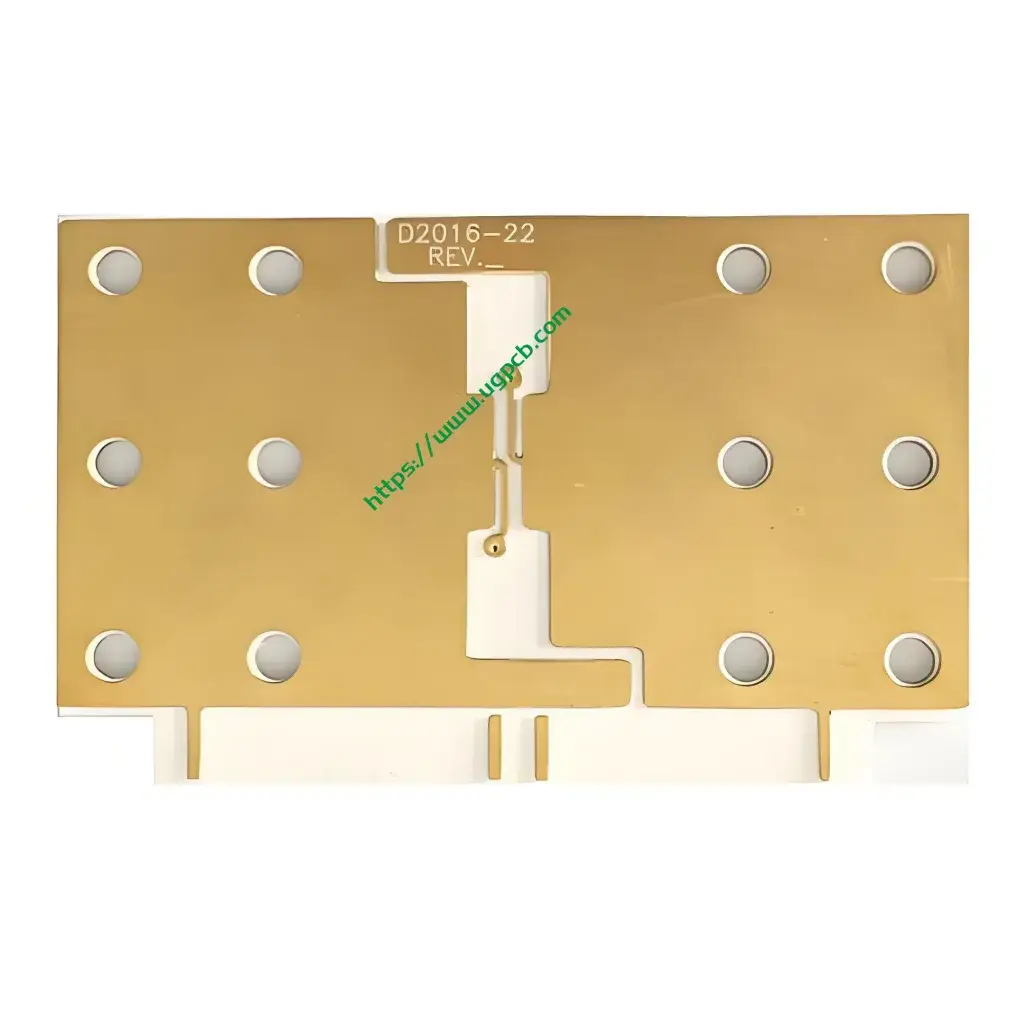
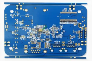
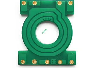
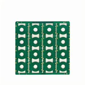
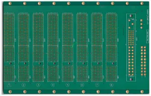
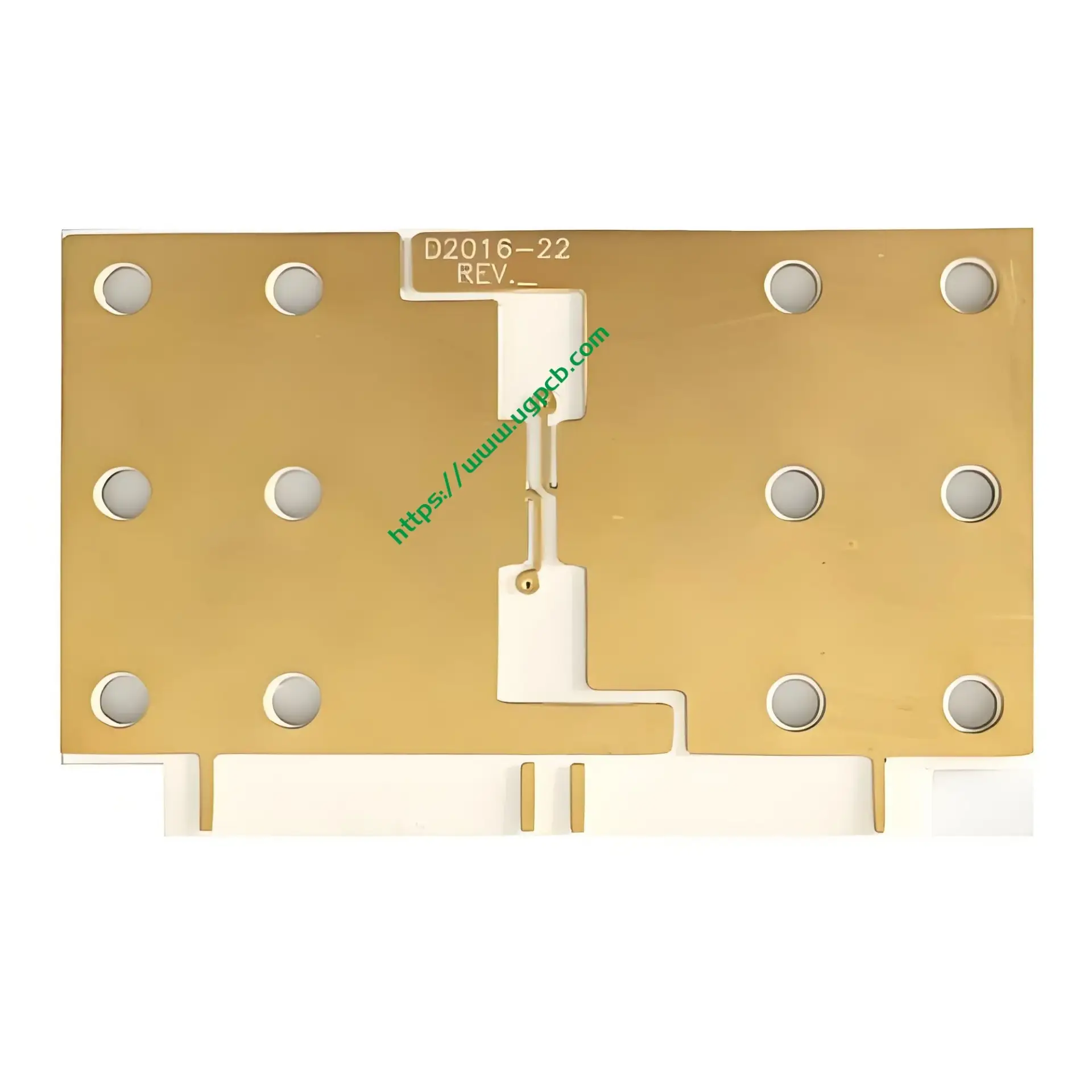
The AlN Ceramic PCB is a high-performance electronic component made from a combination of Ceramic PCB and Ceramic Substrate materials. The Ceramic Substrate, specifically Aluminum Nitride (AlN), serves as the base layer, providing exceptional thermal conductivity and mechanical stability.
Caractéristiques de performance
This PCB stands out for its superior thermal management capabilities, thanks to the AlN Ceramic Substrate. With a PCB thickness of 1.0mm, it offers a balance of durability and flexibility. The Copper Thickness of 1OZ (35un) ensures efficient heat dissipation and high current carrying capacity. The white color of the PCB not only adds to its aesthetic appeal but also reflects heat, further enhancing its thermal performance.
Distinctive Features
The Immersion Gold surface treatment, with a Gold thickness of >=3U”, provides excellent corrosion resistance and electrical conductivity. The 2Layer Ceramic PCB design allows for more complex circuit integration while maintaining a compact footprint. The Minimum aperture of 0.8mm accommodates larger components and higher current densities, making it suitable for high-power applications.
Processus de production
The production of AlN Ceramic PCB involves a multi-step process. Initially, the AlN Ceramic Substrate is prepared and precision-cut to the desired dimensions. Suivant, copper foil is laminated to the substrate, achieving the specified Copper Thickness. Circuits are etched onto the copper foil using advanced photolithography and etching techniques, according to the required circuit design. The final step involves applying the Immersion Gold surface treatment to enhance corrosion resistance and electrical conductivity, resulting in a finished PCB with a thickness of 1.0mm.
Scénarios d'application
The AlN Ceramic PCB finds diverse applications across various industries. In the communication sector, it supports high-frequency antennas and signal processing units. Automotive power control modules and AC converters leverage its thermal stability and high power handling capabilities. It is also widely used in dimming systems, allumeurs, DC-AC converters, switching machines, relais statiques, and rectifier bridges. En plus, its high thermal conductivity makes it an ideal choice for high-power LEDs and other heat-sensitive components.
 LOGO UGPCB

