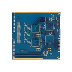
PCB de la station de base de communication: An In-Depth Overview
The Communication Base Station PCB is an advanced electronic component specifically designed for communication base stations. This PCB plays a crucial role in ensuring efficient and reliable communication by providing a stable platform for various electronic components and circuits.
Definition and Purpose
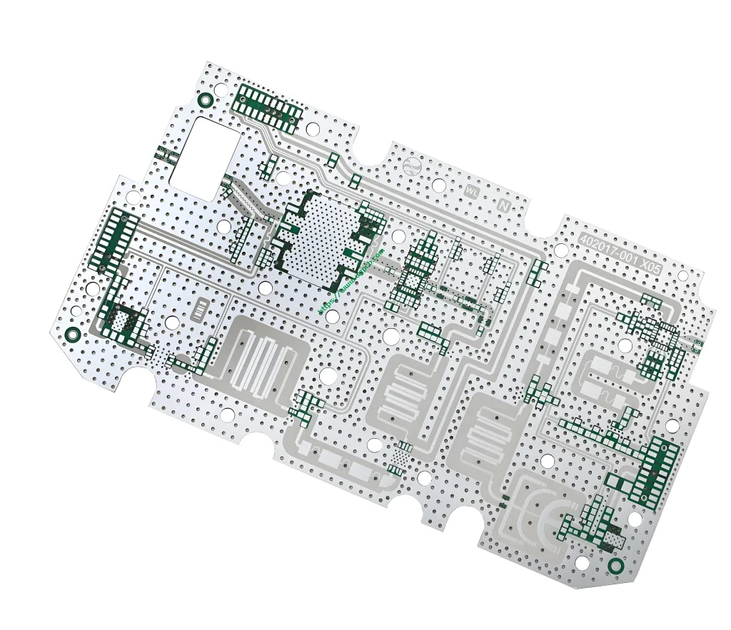
A Communication Base Station PCB, ou carte de circuit imprimé, is a complex assembly of interconnected electronic components used in communication base stations. Its primary function is to facilitate the transmission and reception of signals while maintaining signal integrity and minimizing interference.
How It Works
The Communication Base Station PCB operates on the principle of electrical connectivity and signal routing. It uses conductive pathways, known as traces, to connect different electronic components. These traces are etched onto a non-conductive substrate, creating a network that allows electricity to flow where needed.
Applications
Communication Base Station PCBs are primarily used in telecommunication infrastructure. They are essential in base stations for mobile networks, communications par satellite, and other forms of wireless communication systems. These PCBs ensure that data is transmitted efficiently and reliably between devices.
Types of Communication Base Station PCBs
There are various types of Communication Base Station PCBs, each designed for specific applications and performance requirements. Some common types include single-sided, double face, multilayer, and flexible PCBs. The choice of type depends on factors such as signal complexity, space constraints, and cost considerations.
Composition des matériaux
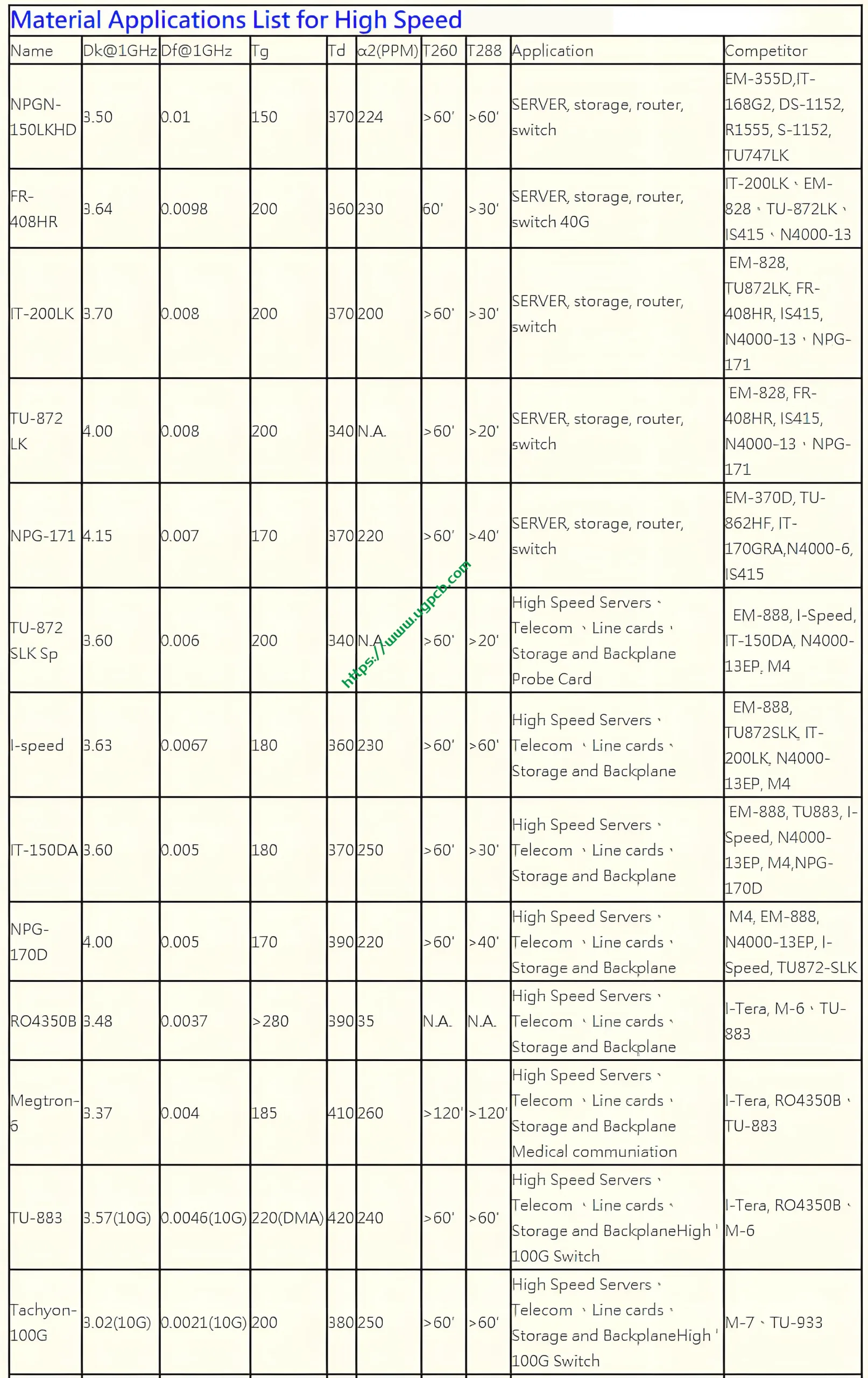
The material used for Communication Base Station PCBs is typically TU883, which is a high-performance laminate material suitable for demanding applications. This material provides excellent thermal stability, résistance mécanique, and dielectric properties, making it ideal for use in communication base stations.
Caractéristiques de performance
The Communication Base Station PCB boasts several key performance characteristics:
- Épaisseur: The finished thickness of the PCB is 1.8mm, providing a robust structure capable of supporting heavy components.
- Épaisseur du cuivre: With a copper thickness of 1OZ (ounce), the PCB offers excellent electrical conductivity and durability.
- Traitement de surface: The surface is treated with immersion gold, enhancing solderability and corrosion resistance.
- Trace and Space: The minimum trace and space are both 4mil (0.1mm), allowing for fine detail and high-density circuitry.
Caractéristiques structurelles
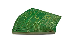
The structural design of the Communication Base Station PCB includes multiple layers, typically 16 couches, to accommodate complex circuit designs and minimize signal interference. The green/white color scheme aids in visual inspection and troubleshooting.
Avantages
Some of the notable advantages of the Communication Base Station PCB include:
- Haute fiabilité: The use of premium materials and advanced manufacturing techniques ensures long-term reliability and performance.
- Signal Integrity: The multilayer design and precise trace routing help maintain signal integrity, even at high frequencies.
- Durability: The thick copper layer and robust substrate provide physical durability, able to withstand harsh environmental conditions.
Processus de production
The production process of a Communication Base Station PCB involves several stages:
- Conception: Using specialized software, the PCB layout is designed with precision.
- Préparation des matériaux: High-quality TU883 material is prepared for layering.
- Gravure: Conductive pathways are etched onto the substrate using chemical processes.
- Layering: Multiple layers are bonded together to form a multilayer PCB.
- Traitement de surface: The surface is treated with immersion gold for enhanced properties.
- Essai: Each PCB undergoes rigorous testing to ensure it meets quality standards.
- Finishing: Final touches are added, including silk screening and coating.
Use Case Scenarios
The Communication Base Station PCB is used in a variety of scenarios within telecommunication infrastructure:
- Mobile Networks: Ensuring seamless connectivity in cellular towers and base stations.
- Communications par satellite: Supporting ground station operations for satellite data transmission.
- Military Communications: Providing reliable communication links in defense applications.
- Emergency Services: Enabling efficient communication during disaster response and recovery operations.
En conclusion, the Communication Base Station PCB is an indispensable component in modern telecommunication systems, offering high performance, fiabilité, et durabilité. Its sophisticated design and advanced materials make it suitable for a wide range of applications, ensuring efficient and uninterrupted communication.
 LOGO UGPCB

