
Overview of Multilayer Golden Finger PCB for USB Connector
The multilayer golden finger PCB for USB connector is a specialized product designed to meet the stringent requirements of USB applications. Ce type de PCB offre une haute précision, fiabilité, et les performances, making it an ideal choice for various USB-related devices.
Définition
A multilayer golden finger PCB for USB connector is a printed circuit board specifically designed to support the functions of a USB connector. Il se compose de plusieurs couches de matériaux conducteurs et isolants, providing complex electrical pathways and connections essential for the operation of the USB connector.
Exigences de conception
When designing a multilayer golden finger PCB for USB connector, Plusieurs exigences clés doivent être satisfaites:
- Material Quality: High-quality FR4 material is essential for durability and signal integrity.
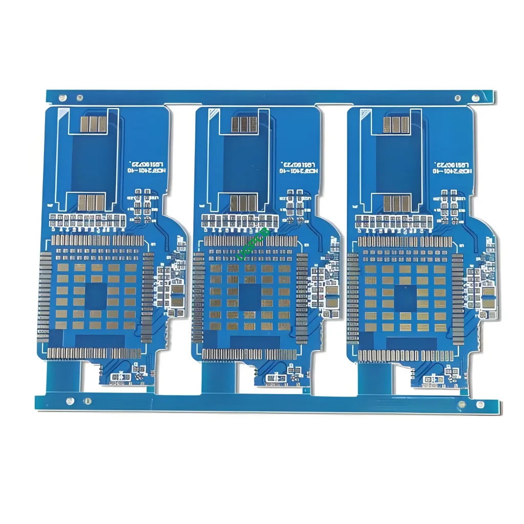
- Layer Configuration: A 6-layer design is standard, allowing for complex circuitry and signal routing.
- Épaisseur du cuivre: A copper thickness of 1OZ ensures adequate conductivity.
- Traitement de surface: Immersion gold surface treatment enhances connectivity and corrosion resistance.
- Trace/Space Dimensions: Minimum trace and space dimensions of 4mil (0.1mm) are required for precise circuit patterns.
- Special Features: Golden finger PCB design is often incorporated for specific component placement and soldering requirements.
Principe de fonctionnement
The multilayer golden finger PCB for USB connector operates based on the principles of electrical conductivity and insulation. Conductive layers form the pathways for electrical signals, while insulating layers prevent unwanted interactions between these signals. Le traitement de surface d'or à l'immersion offre une excellente connectivité et protège contre les facteurs environnementaux.
Applications
This type of PCB is primarily used in USB connectors, which are crucial components in various electronic devices such as computers, téléphones portables, and peripherals. Ceux-ci incluent:
- USB charging cables
- Data transfer cables
- USB hubs and adapters
- Devices with USB ports
Classification
Multilayer golden finger PCBs for USB connectors can be classified based on their specific features and intended use, tel que:
- Data Transfer Boards: For handling high-speed data transfer in USB connections.
- Power Supply Boards: To manage power distribution in USB-powered devices.
- Tableaux de contrôle: Pour gérer et contrôler diverses fonctions dans les systèmes électroniques.
Matériels
The primary materials used in the construction of a multilayer golden finger PCB for USB connector include:
- Matériau de base: FR4, a flame-retardant fiberglass material known for its excellent dielectric properties and mechanical strength.
- Conductive Material: Cuivre, used for the conductive traces.
- Traitement de surface: L'or d'immersion, which enhances connectivity and provides corrosion resistance.
Performance
The performance of a multilayer golden finger PCB for USB connector is characterized by:
- High Signal Integrity: Due to precise trace/space dimensions and quality materials.
- Reliable Connectivity: Ensured by the immersion gold surface treatment.
- Durability: Enhanced by the robust FR4 base material.
- Electrical Efficiency: Minimized signal loss and interference due to optimized layer configuration.
Structure
The structure of a multilayer golden finger PCB for USB connector consists of:
- Six Layers of Conductive Material: Alternating with insulating layers.
- Immersion Gold Surface Treatment: For enhanced connectivity and protection.
- Golden Finger Design: For specific component placement and soldering requirements.
Caractéristiques
Key features of the multilayer golden finger PCB for USB connector include:
- Advanced Surface Treatment: Immersion gold for superior connection quality.
- High Precision: With minimum trace and space dimensions of 4mil (0.1mm).
- Customizable Color Options: Disponible en vert ou blanc.
- Standard Thickness: Avec une épaisseur finie de 1,0 mm.
Processus de production
The production process for a multilayer golden finger PCB for USB connector involves several steps:
- Préparation des matériaux: Selecting and preparing FR4 sheets and copper foil.
- Empilement de calques: Alternating layers of copper and insulating materials.
- Gravure: Retirer l'excès de cuivre pour former le motif de circuit souhaité.
- Placage: Applying immersion gold surface treatment.
- Laminage: Combining the layers under heat and pressure.
- Forage: Creating holes for through-hole components and vias.
- Solder Mask Application: Protéger le circuit des ponts de soudure et des facteurs environnementaux.
- Sérigraphie: Ajout de texte et de symboles pour le placement et l'identification des composants.
- Contrôle de qualité: Assurer que le PCB répond à toutes les spécifications et normes de conception.
Utiliser des scénarios
The multilayer golden finger PCB for USB connector is ideal for scenarios where:
- Une intégrité élevée du signal est cruciale.
- Des connexions fiables et durables sont nécessaires.
- Les contraintes d'espace nécessitent une conception compacte et efficace.
- Un traitement de surface avancé est nécessaire pour des performances améliorées.


