Composition des matériaux
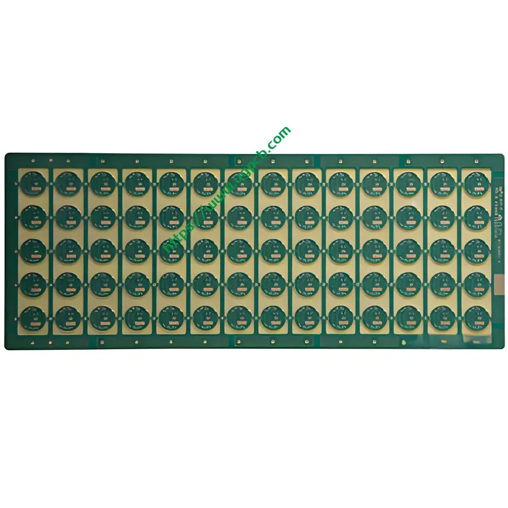
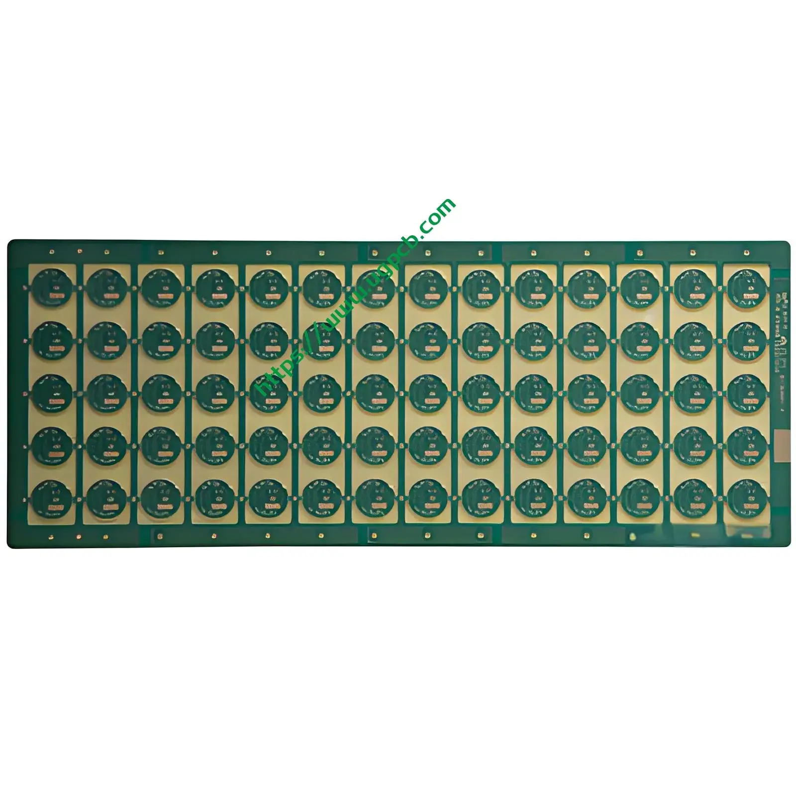
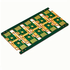
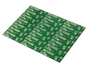
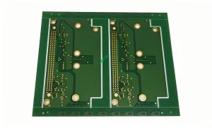
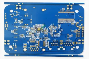
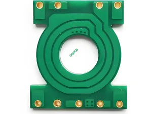
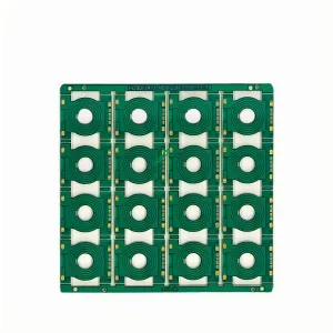
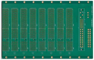
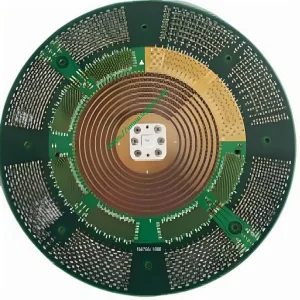
The Aluminum Nitride Ceramic PCB is crafted from a combination of Ceramic PCB and Ceramic Substrate materials. This blend leverages the exceptional properties of both ceramics and PCBs, ensuring a robust and reliable product.
Performance and Characteristics
- Layer Structure: The PCB features a 2-layer design, offering more flexibility and complexity in circuit design.
- Couleur: The white color of the PCB provides a clean and professional appearance.
- Épaisseur: The aluminum nitride layer measures 0.635mm, ensuring a sturdy foundation for your electronic components.
- Épaisseur du cuivre: With a copper thickness of 1OZ (35un), the PCB offers excellent electrical conductivity and current carrying capacity.
- Traitement de surface: The immersion gold surface treatment not only enhances the aesthetic appeal but also provides corrosion resistance and ensures smooth soldering.
- Épaisseur de l'or: The gold thickness of >=3U” further reinforces the corrosion resistance and soldering quality.
- Ouverture minimale: The minimum aperture of 0.8mm allows for the precise placement of small components, making it suitable for high-density packaging.
Unique Features
- Grâce à la technologie des trous: This allows for the creation of vias and interconnections between different layers, enhancing the PCB’s functionality.
- Ceramic Dam Technology: This innovative technology ensures precise alignment and sealing of holes, preventing any leakage and enhancing the PCB’s reliability.
Processus de production
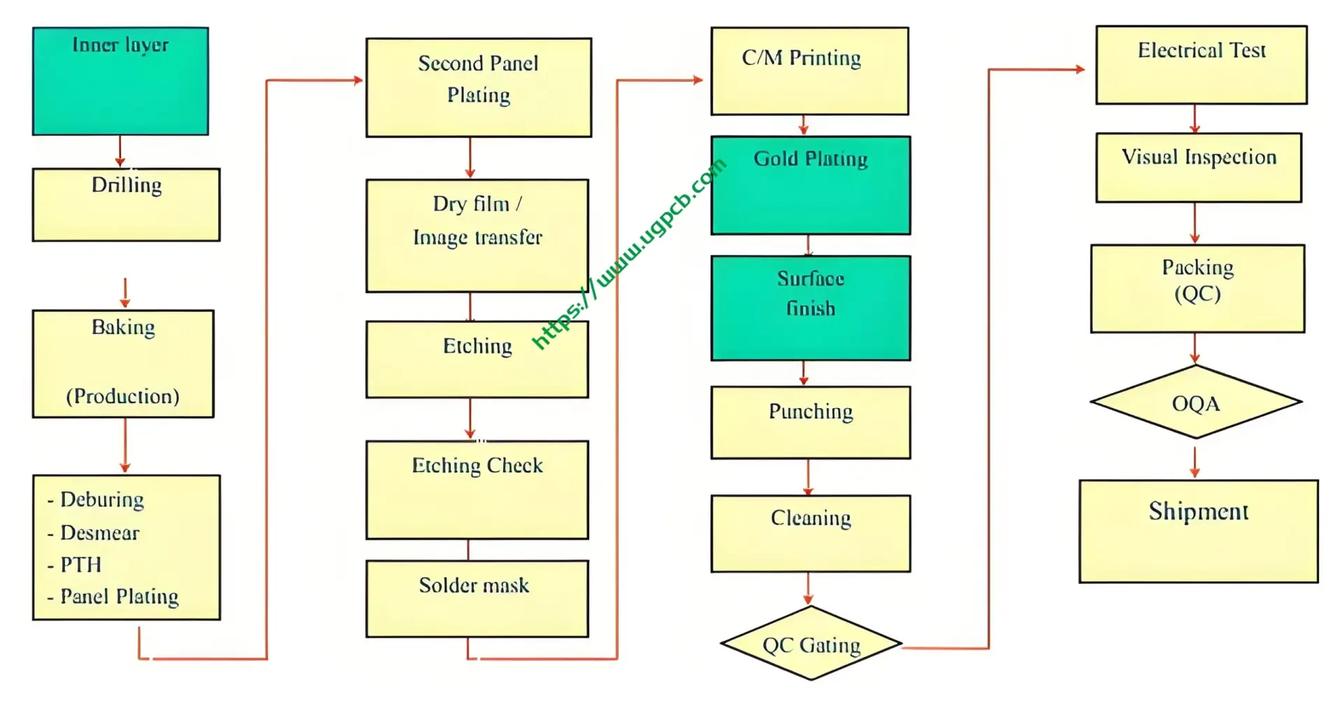
The production of Aluminum Nitride Ceramic PCBs involves several meticulous steps:
- Préparation des matériaux: High-quality aluminum nitride powder and ceramic substrate materials are carefully selected and prepared.
- Layer Formation: The ceramic substrate is bonded with the aluminum nitride layer to form the PCB’s base structure.
- Modèle de circuit: Using advanced etching techniques, the desired circuit patterns are etched onto the copper layer.
- Through Hole Creation: Precision drilling techniques are used to create through holes for interconnections.
- Ceramic Dam Application: Ceramic dam technology is applied to ensure the precise alignment and sealing of holes.
- Traitement de surface: The PCB undergoes immersion gold plating to provide a corrosion-resistant and soldering-friendly surface.
- Contrôle de qualité: Rigorous testing and quality control measures are implemented to ensure the PCB meets all specifications and standards.
Scénarios d'application
Aluminum Nitride Ceramic PCBs are ideal for a wide range of applications:
- High-Power Electronics: Their excellent thermal conductivity and high-temperature resistance make them suitable for use in high-power electronic devices.
- Circuits haute fréquence: Their low loss and high stability make them perfect for high-frequency circuits, such as those used in wireless communications.
- Dispositifs médicaux: Their durability and reliability make them ideal for use in medical equipment that requires precise and consistent performance.
- Industrial Applications: Their robust design and high-temperature tolerance make them suitable for use in harsh industrial environments.
En résumé, the Aluminum Nitride Ceramic PCB combines exceptional material properties, advanced manufacturing techniques, and versatile application scenarios, making it an ideal choice for high-performance electronic devices.
 LOGO UGPCB

