RO4450F vs RO4450T
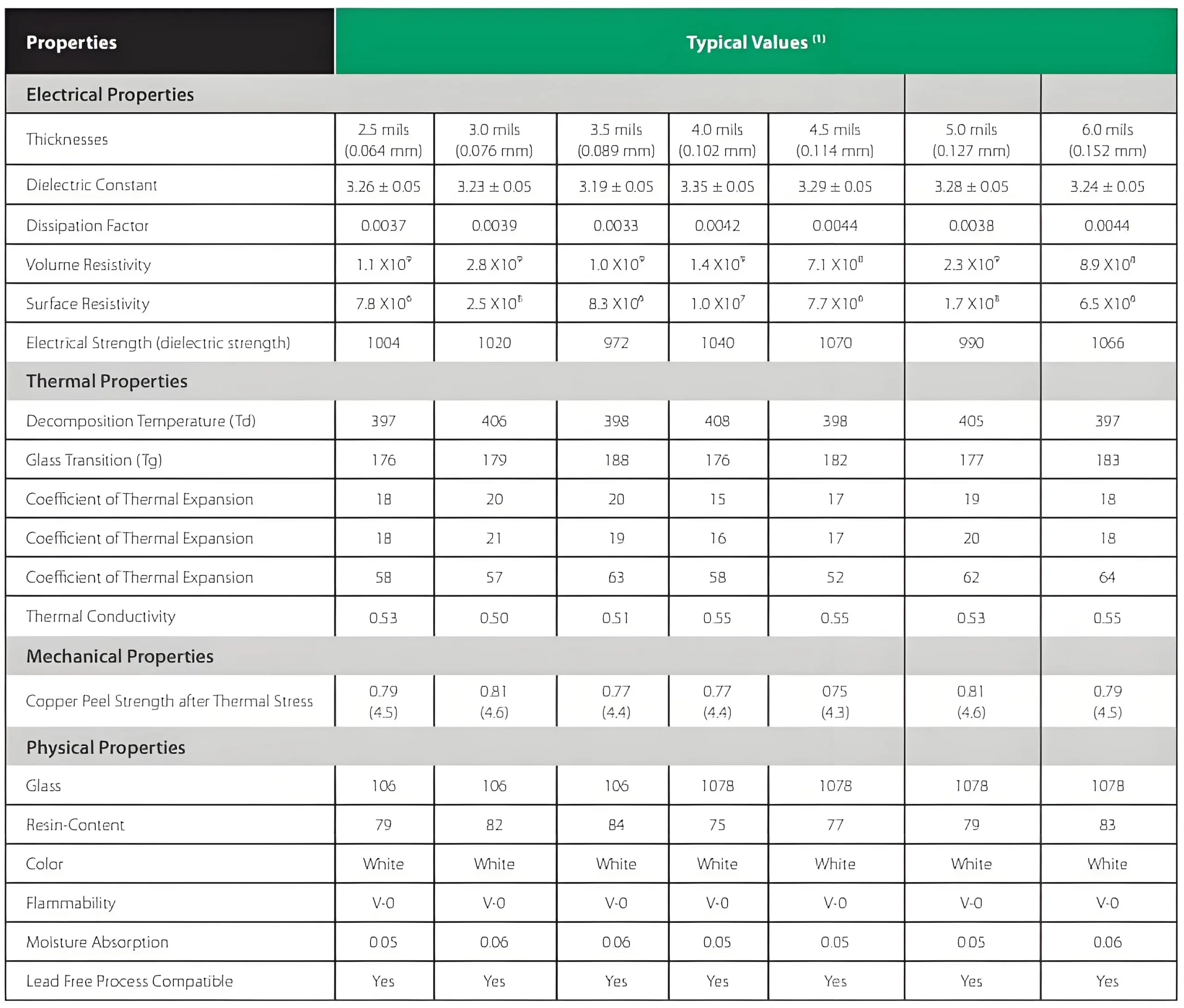
RO4450T (constante diélectrique 3.23, thickness 3mil, loss factor 0.0039; constante diélectrique 3.35, thickness 4mil, loss factor 0.004,; constante diélectrique 3.28, thickness 5mil, loss factor 0.0038).

Rogers RO4450T PCB material
RO4450F (constante diélectrique 3.52, loss factor 0.004, thickness 4mil). The expansion coefficient and volume resistivity of the other two materials are different.
Rogers RO4450T can achieve a thinner thickness of 3mil. RO4450T has three specifications of 3mil, 4mil, and 5mil. The dielectric constant is 3.23, 3.35, et 3.28, while the RO4450F is only 4mil, and the dielectric constant is 3.52.
Rogers Corporation Advanced Attachment Solutions (ACS) is currently experiencing a surge in demand for the RO4450T, un 3 mil thick bond sheet. This surge consumes specific raw materials at a faster rate than general consumption. To provide our customers with up-to-date information so they can plan. RO4450T 3 mil thickness orders for 3 mil thickness provisional manufacturing lead times at Rogers’ Arizona facility extended from ≤ 12 business days to ≤ 17 business days from receipt of order working days.
This temporary lead time extension applies only to the RO4450T 3 mil bond sheet. The RO4450T’s lead-time bond plies of 2.5, 3.5, 4, 4.5, 5, et 6 mils remain unchanged.
Rogers models
RO4400、RO4450B、RO4450F、RO4450T、RO4460G2、RO4003C、RO4350B、RO4360G2、RO4835、RO4835T、RO4000 LoPRO、RO4400、RO4000、RO4450B、RO4450F、RO4460G、RO4003C、RO4350B、RO4360G2、RO4450T、RO4460G2、RO4835、RO4835T、4450B、4450F , 4450T, 4460G2
The RO4400 series of prepregs are based on RO4000 substrate material and are compatible with RO4000 sheets in a multi-layer construction. RO4400 series products have a high glass transition temperature, and their fully cured prepregs do not thermally degrade during multiple laminations, making them the first choice for the continuous production of multi-layer board materials. En outre, the lower lamination temperature and controllable glue flow compatible with FR4 enable the RO4400 prepreg and FR4 prepreg in the multi-layer board to be completed by one lamination.
RO4450F prepreg has improved lateral flow properties compared to RO4450B and has become the first choice for new designs or an alternative when filling is difficult in designs. RO4460G2 prepreg is a 6.15 constante diélectrique (Ne sait pas) prepreg bonding material that, like other RO4400 series prepreg materials, has excellent dielectric constant tolerance control, while a low z-axis expansion coefficient ensures smooth hole reliability. RO4450T prepreg has similar lateral flow properties as RO4450F prepreg. It is a prepreg reinforced with fiberglass cloth. It provides designers with a variety of thicknesses to choose from, and its flexibility is also necessary for high-level circuit design.
Each prepreg in the RO4400 series has UL-94 flame retardant certification and is suitable for lead-free processing.
Characteristics of RO4400 series materials: CAF resistance (Ion migration resistance)

The parameters of Rogers RO4450T PCB material.
PCB Material Storage
RO4835T Laminate and RO4450T Bond Sheet, when both sides are metalized, can be stored at room temperature (50-90°F/10-32°C). Suggest
UN “first in, first out” inventory system is used, and the lot number of the sheet is recorded from the PWB process to the delivery of the finished product.
PCB inner layer production
RO4835T sheet is compatible with various alignment systems. Select the corresponding alignment hole, such as round or square, according to the ability to process long lengths and the alignment requirements of the product
Dowel pins, standard or multi-row locating holes, punching before or after etching, etc.. Usually square locating pins are matched with multiple rows of locating holes.
can meet the needs of most customers.
Surface treatment and etching process of PCB graphic transfer
The chemical process used in the pretreatment of pattern transfer usually includes steps such as cleaning, micro-etching, water washing and drying. According to the thickness after pressing, the mechanical grinding plate
The method can also be used for the surface treatment of the secondary outer core board after lamination.
RO4835T sheet is compatible with most liquid photosensitive films and dry films. After the pattern is transferred, it can be developed, etched and stripped in the same way as FR-4.
(DES pull) and other production processes. In order to improve the alignment control of multilayer boards, the OPE punching process is the first choice.
PCB oxidation treatment
The RO4835T sheet can be compatible with any oxidation or oxidation substitution method to treat the copper foil surface. According to the thickness of the core board and the capacity of the equipment,
Pull plate supports may be used when very thin inner cores pass through horizontal oxidation lines.
PCB pressing
RO4835T sheet is compatible with any RO4400 adhesive sheet, but it is better to match and press with RO4450T adhesive sheet. in order to achieve the best
Layer copper foil adhesion, need to use CU4000 & CU4000 LoPRO copper foil to match, CU4000 & CU4000 LoPRO copper foil can
Purchased from Rogers Corporation, it is suitable for all copper-laminated multilayer constructions.
PCB Drilling
The RO4835T core board and the multi-layer board laminated with the RO4450T bonding sheet are suitable for making micro-blind holes and through holes by UV and CO2 laser processes. And for
Mechanical drilling, whether it is the RO4835T core board and the multi-layer board made from the RO4835T core board, it is recommended to use a standard cover plate (aluminum sheet or thin phenolic
board) and backing board (phenolic board or high-density fiberboard) material.
Although the drilling operation window of RO4835T/RO4450T is very wide, it is necessary to avoid the drill speed exceeding 500SFM;
Diameter: 0.0135” – 0.125”) and large drills (greater than 0.125” diameter), the recommended infeed is more than 0.002”; but for small drills (diameters greater than 0.125”)
less than 0.0135”), the feed amount should be less than 0.002”. En général, standard drills are more efficient at removing cuttings than undercut drills. Drill life
The fate needs to be determined by the quality of the PTH, not the appearance of the drill. Drilling RO4000 sheet will accelerate the wear of the drill, but the roughness of the hole wall is determined by the ceramic
The particle size distribution determines, not the degree of wear on the drill. The same drill, from the first hole to several thousand holes, the hole wall roughness is usually maintained at
8-25µm.
PTH process
Traitement de surface: Choose according to thickness, thick sub-layer and outer layer board can use nylon brush to clean copper surface. Thin boards may require manual brushing, sandblasting
Or chemical treatment for surface treatment. En général, it is necessary to choose the most appropriate method to drape and copper according to the thickness and size of the board.
PCB surface treatment
Due to the high glass transition temperature and low resin content of the resin, excessive chemical and plasma debinding of the drilled holes is generally not required. like
If inspection is required to determine the quality of the drilled holes, a shortened chemical stripping process should be considered (approximately half of the FR4 standard Tg material)
time). Such as reducing bulk and potassium permanganate tank processing time, but may need to extend the processing time in the neutralization tank. In processing products with CAF requirements
When the glue is not removed, or CF4/O2 plasma glue removal is the first choice.
Like RO4000 series boards, we do not recommend using etch back process on RO4835T double-sided boards and multi-layer boards made with RO4450T. over
The etch back will loosen the filler on the hole wall, a large amount of etch back will appear in the LopRO resin layer, and the chemical solution will seep in and out along the glass cloth
The wick effect is present.
PCB metallization holes
The RO4835T and RO4450T sheets do not require special treatment before metallization, and it can use electroless copper or direct copper plating. for tall
For boards with diameter ratio through holes, it is recommended to do a quick copper plating (thickness 0.00025”) before the pattern transfer.
PCB copper plating and outer layer processing flow:
The RO4835T and RO4450T multi-layer boards can use the board and pattern plating process, using standard copper and tin plating processes. After electroplating, in conventional
The SES production line etched patterns (film stripping, etching and tin stripping).
The surface of the etched medium should be protected, and the better green oil adhesion can be satisfied after the green oil direct silk screen printing and the green oil imaging transfer.
PCB Final Metal Finish
The RO4835T and RO4450T are compatible with OSP, HASL, and most chemical deposition or surface plating processes.
PCB shape processing
The multi-layer board made of RO4835T core board and RO4450T bonding sheet can be cut, sawed, trimmed, milled, stamped and laser squared, respectivement.
shape processing. For multi-unit panels, V-grooves and stamp holes can be designed between the circuit board units, so that the single unit can be easily assembled after automatic assembly.
Circuit board separation.
PCB milling board
The tungsten carbide tools and processing conditions used to mill RO4000 laminates and multi-layer boards are similar to traditional epoxy materials (FR-4). To avoid copper cape
The production requires etching the copper at the position of the milling cutter.
PCB maximum stack height
The maximum stack height is 70% of the effective edge length of the tool to facilitate chip evacuation
PCB milling cutter type
Tungsten carbide multi-blade milling cutter or diamond cutter.
PCB milling conditions
To prolong tool life, the surface speed needs to be less than 500SFM. Typically more than 30 feet of tool life at maximum stack thickness
Life.
Cutting Amount: 0.0010-0.0015” (0.0254-0.0381mm)/rev
Surface Speed: 300 – SFM
 LOGO UGPCB


