
PCB Stackup Design
Nel design elettronico moderno, PCB (Circuito stampato) Stackup Design è uno dei fattori chiave che determinano le prestazioni del circuito, affidabilità, and cost. Especially when the number of layers exceeds four, stackup design not only affects signal integrity, electromagnetic compatibility (EMC), and thermal management but also directly impacts manufacturing costs and process complexity. This article will start with fundamental concepts, delve into the core principles of Circuito stampato stackup design, material selection, and high-speed signal optimization strategies, helping engineers make more informed decisions during the design process.
Fundamentals of PCB Stackup Design
What is PCB Stackup?
PCB stackup refers to the process of stacking multiple layers of copper-clad cores (Core), prepreg (Prepreg, abbreviated as PP), and copper foil in a specific sequence, which are then laminated to form an integrated multilayer circuit board struttura. The core of stackup design lies in the rational allocation of signal layers, power layers, and ground layers to meet electrical performance, resistenza meccanica, and cost control requirements.
For single or double-layer boards, stackup design is relatively simple, typically requiring only the selection of appropriate copper-clad board thickness and copper weight. Tuttavia, when designing multilayer boards with four or more layers, stackup design becomes complex and critical. Per esempio, the stackup design of a 16-layer board must consider signal integrity, impedance control, EMC shielding, thermal management, e altri fattori.
Key Materials in Stackup Design
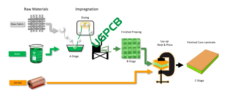
The manufacturing process of the PCB core board.
- Copper-Clad Core (Core): Composed of insulating substrate (such as epoxy resin, fiberglass) e lamina di rame, providing mechanical support and electrical insulation.
- Prepreg (Prepreg): Made of fiberglass cloth impregnated with epoxy resin, used for interlayer bonding and insulation.
- Lamina di rame: Used to form conductive traces, with common thicknesses of 0.5oz (18μm), 1oz (35μm), and 2oz (70μm).
Core Principles of PCB Stackup Design
Layer Allocation and Signal Integrity
When designing multilayer PCBs, the number of layers must first be determined based on circuit scale and EMC requirements. Typically, signal layers, power layers, and ground layers should be alternately distributed to reduce signal crosstalk and electromagnetic interference. Per esempio, for high-speed signals, UN “GND/Signal/GND” stackup combination is recommended to minimize crosstalk coupling.
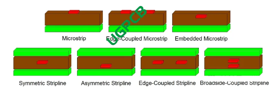
Type of Microstrip and Stripline Routing
- Stripline: Suitable for critical high-speed signals, where the signal line is sandwiched between two ground planes, providing excellent shielding.
- Microstrip: Suitable for non-critical high-speed signals, where the signal line is on the outer layer, offering flexible routing but poorer shielding.
Impedance Control
Impedance control is one of the core aspects of high-speed PCB design. Common single-ended impedance is 50Ω, and differential impedance is 100Ω. Impedance mismatch can cause signal reflection, distortion, and radiation, affecting signal integrity. Key parameters for impedance control include:
- Trace Width and Spacing: Primary factors affecting impedance.
- Costante dielettrica: Materials with low dielectric constants help reduce signal delay and loss.
- Spessore del rame: Inner signal layers typically use 0.5oz copper thickness to meet precise etching requirements.
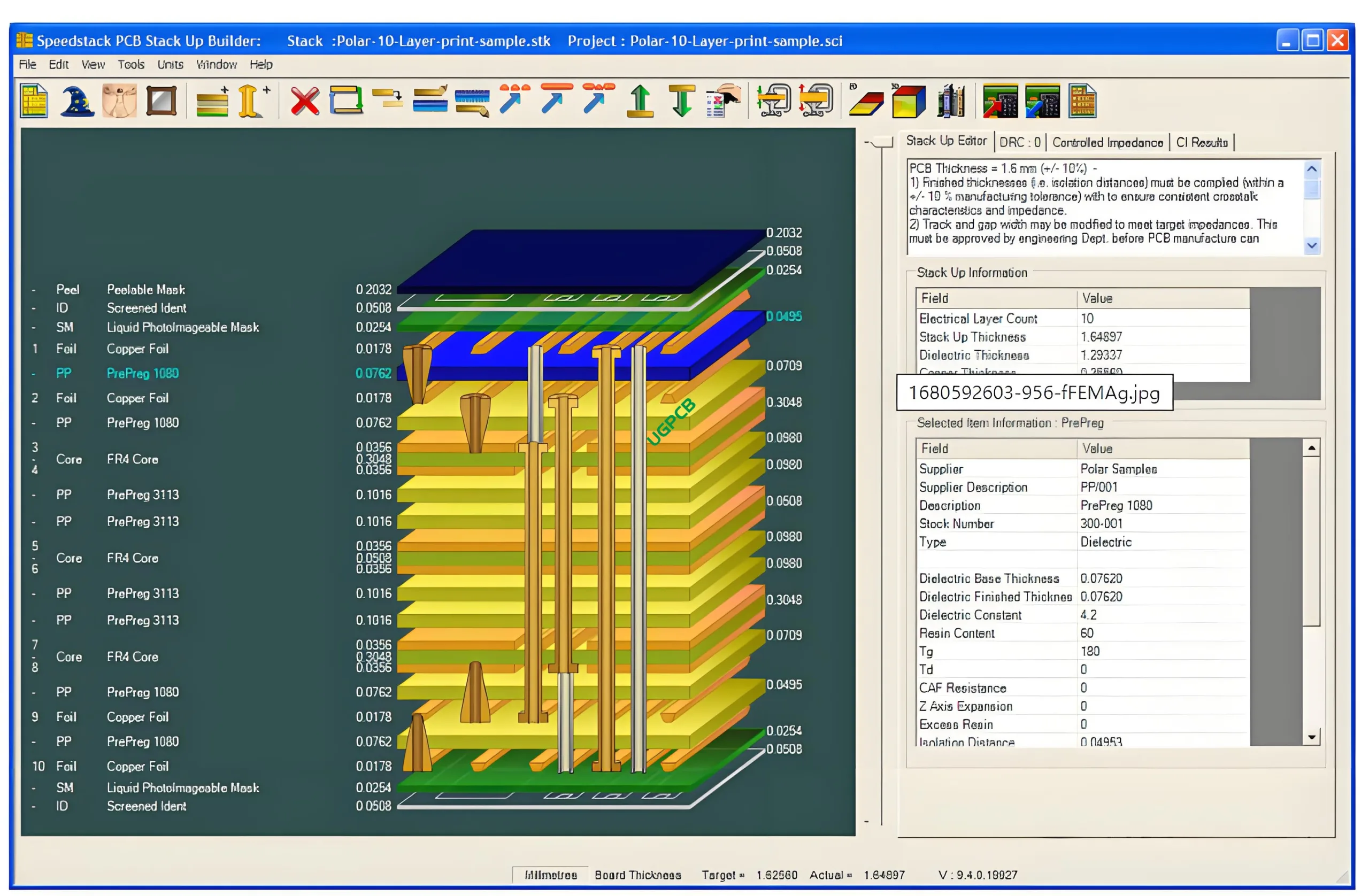
PCB Board Stack-Up Impedance Control
EMC Design
The goal of EMC design is to reduce electromagnetic interference (EMI) and enhance anti-interference capabilities. Some basic principles include:
- Adjacent Power and Ground Layers: Utilize interlayer capacitance as a power smoothing capacitor while shielding radiation currents.
- Routing Layers Adjacent to Power or Ground Layers: Reduce interference through flux cancellation.
- Ground Plane as a Shield Layer: Suppress common-mode RF interference and reduce the distribution impedance of high-frequency power.
Optimization Strategies for High-Speed PCB Stackup Design
Material Selection
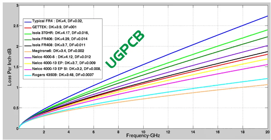
Attenuation of signals by different types of materials.
High-speed PCBs require materials with low loss tangent (Df) and low dielectric constant (Non so). Common FR-4 materials are suitable for most applications, but for high-speed scenarios, high-performance materials such as Panasonic’s Megtron4/6 series are recommended. Per esempio, Megtron6 exhibits a signal loss of only 0.85dB/inch at 28Gbps, while FR-4 has a loss of up to 2dB/inch.
Fiberglass Effect and Copper Foil Roughness
Surface Roughness of Copper Foils with Different Grades
- Fiberglass Effect: The weaving style of different fiberglass cloths affects signal characteristics. To mitigate the fiberglass effect, choose fiberglass types with minimized resin windows or use Zig-Zag routing methods.
- Copper Foil Roughness: In high-speed signal design, copper foil surface roughness affects signal transmission. Its impact is minimal below 5GHz but becomes significant above 10GHz.
Thermal Management
High-speed PCBs often come with high power consumption, making thermal management crucial. Some optimization strategies include:
- Selecting High Thermal Conductivity Materials: Such as metal-based substrates (aluminum or copper).
- Designing Thermal Pads and Vias: Improve heat conduction efficiency.
- Increasing Ground Planes and Copper Pour Areas: Enhance heat dissipation capabilities.
Practical Applications of PCB Stackup Design
16-Layer Board Stackup Design

16-Layer Board Stackup Design
Taking a 16-layer board as an example, a typical stackup structure is as follows:
- Top Layer (Signal Layer)
- Ground Layer
- Signal Layer
- Power Layer
- Signal Layer
- Ground Layer
- Signal Layer
- Core Layer
- Signal Layer
- Ground Layer
- Signal Layer
- Power Layer
- Signal Layer
- Ground Layer
- Signal Layer
- Bottom Layer (Signal Layer)
This structure effectively reduces crosstalk and electromagnetic interference by alternately distributing signal and ground layers while meeting the impedance control requirements of high-speed signals.
Via Structure Design
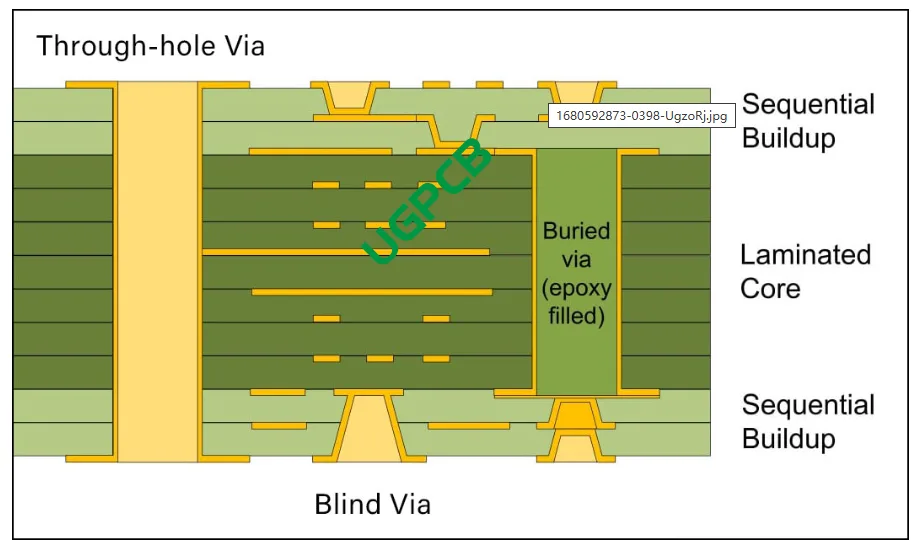
PCB Board Hole Types
In HDI PCBs, blind vias and buried vias are widely used to optimize routing space. Tuttavia, these via structures increase manufacturing difficulty and cost. Perciò, via structures should be simplified during design, such as prioritizing through-hole vias (PTH).
Conclusione
PCB stackup design is a complex and critical task involving material selection, layer allocation, impedance control, EMC design, and thermal management. Through rational stackup design, circuit performance and reliability can be improved while effectively controlling costs. For high-speed PCB design, selecting low-loss materials, optimizing fiberglass effects and copper foil roughness, and strengthening thermal management are key to ensuring signal integrity and stability.
Whether you are a beginner or a seasoned engineer, mastering the core principles and optimization strategies of PCB stackup design will lay a solid foundation for the successful design of electronic products.
