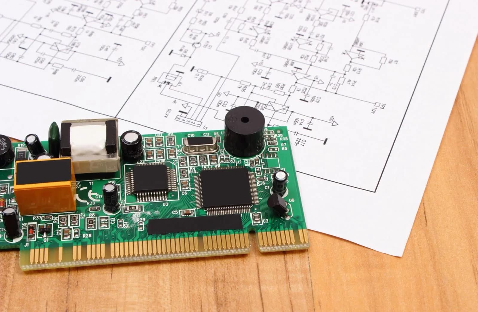
Progettazione PCB RF
RF PCB Design Solutions: A Professional Platform Empowering High-Frequency Applications
Core Challenges and Value of High-Frequency Circuit Design
In fields such as wireless communication, sistemi radar, navigazione satellitare, and 5G/6G devices, RF PCB design is the core technology that determines signal integrity, power transmission efficiency, and system reliability. The primary challenges include:
- High-Frequency Signal Loss Control: Effetto della pelle, Perdita dielettrica, and impedance mismatch become significant at GHz frequencies.
- Compatibilità elettromagnetica (EMC) Ottimizzazione: Reducing crosstalk and radiation to meet stringent certification standards like FCC and CE.
- 3D Electromagnetic Field Co-Design: Addressing field distribution optimization for transmission line structures such as microstrips and coplanar waveguides.
- Thermal-Mechanical-Electrical Multi-Physics Coupling: Balancing heat dissipation and mechanical stability in high-power scenarios.
As a core competency, UGPCB is committed to helping clients achieve key performance indicators such as insertion loss ≤0.3dB/inch (@28GHz), VSWR <1.5, and phase consistency of ±2° through full-process simulation verification and process innovation.
La nostra matrice di capacità professionale: From PCB Material Selection to Manufacturing
High-Frequency Material Selection and Characterization
- Libreria di materiali dielettrici: Covers high-frequency laminates like Rogers RO4000® series, Taconic TLY, and Isola I-Tera® MT, with dielectric constants (Non so) che vanno da 2.2 A 10.2 and loss tangents (Df) as low as 0.0015.
- Copper Foil Treatment: Combines ultra-low profile copper (RTF/VLP) with brown oxide treatment to achieve surface roughness Ra <0.3μm.
- Hybrid Dielectric Stackup Design: Supports PTFE and FR-4 hybrid lamination for optimal performance-cost balance.
Precision Impedance Control Design
- Utilizes Sonnet®/HFSS full-wave simulation for multi-impedance system co-design (50Ω/75Ω/100Ω).
- Controls differential pair length tolerance within ±5mil and stripline impedance tolerance within ±5%.
- Features proprietary edge compensation algorithms to eliminate microstrip edge field distortion.
3D Electromagnetic Shielding Architecture
- Implements via fence shielding technology with isolation >60dB @10GHz.
- Designs embedded waveguide structures to suppress surface wave propagation.
- Optimizes RF-digital ground interference through localized ground plane segmentation.
Interconnessione ad alta densità (ISU) Integrazione
- Achieves laser drilling accuracy of ±25μm for blind and buried vias, supporting 0.1mm microvia designs.
- Employs any-layer HDI technology for integrating 20+ layer millimeter-wave antenna arrays.
- Controls gold finger plating thickness at 0.05–0.2μm, ensuring contact resistance <10Mω.
Our Full-Process Technical Support System
To verify the rationality of the design, we also need to conduct rationality checks during the PCB design, produzione, and testing phases. This allows us to identify any issues promptly, ensuring that your product is manufactured safely and undergoes quality control.
Fase di verifica del design
- Electromagnetic Simulation: Extracts S-parameters across full frequency bands using ANSYS HFSS/CST.
- Simulazione termica: Analyzes power device thermal distribution with Flotherm®.
- Reliability Verification: Conducts HALT tests (-55Da ℃ a 150 ℃ ciclismo, 20G Vibrazione).
Controllo dei processi di produzione
- Utilizes laser direct imaging (LDI) technology with line width tolerance of ±8%.
- Employs plasma desmear processes to ensure high-frequency hole wall roughness <1μm.
- Implements vacuum lamination to maintain interlayer dielectric thickness deviation <3%.
Test e certificazione
- Performs vector network analyzer (VNA) testing with frequency coverage from DC to 110GHz.
- Locates EMI radiation sources using near-field scanning systems.
- Conducts comprehensive wireless communication protocol testing (including ETSI EN 300 328 and FCC Part 15).
Scenari di applicazione tipici
- 5G Stazione base AAU: 32T32R Massive MIMO antenna boards supporting n257/n258 millimeter-wave bands.
- Satellite Communication Terminals: Ka-band phased array antennas with EIRP >50DBM.
- Automotive Radar: 77GHz millimeter-wave radar PCBs compliant with AEC-Q200 reliability standards.
- Medical RF Equipment: Dual-frequency integrated designs for 13.56MHz RFID and 6.78MHz WPT.
Modelli di servizio e supporto tecnico
- Prototipazione rapida: Delivers 10-layer RF board samples within 48 ore.
- Design-Simulation-Testing Collaborative Platform: Supports design reviews in ODB++/IPC-2581 formats.
- Failure Analysis Laboratory: Provides in-depth services like TDR fault location and cross-section analysis.
- Industry Certification Support: Complies with ISO 9001/IATF 16949 systems and holds military-grade NADCAP accreditation.
Dal concetto alla produzione di massa
With over 15 years of RF design experience, a database of 200+ casi di successo, we deliver uncompromising high-frequency solutions for your wireless systems.
Contact our expert team today for a customized design evaluation report!


WeChat
Scansiona il codice QR con WeChat