
Introduzione
In blind vias IC substrate proofing, the application of blind holes and buried holes greatly reduces the size and quality of blind vias IC substrate PCB, reduces the number of layers, improves electromagnetic compatibility, increases the characteristics of electronic products, reduces costs, and makes the design work more simple and fast.
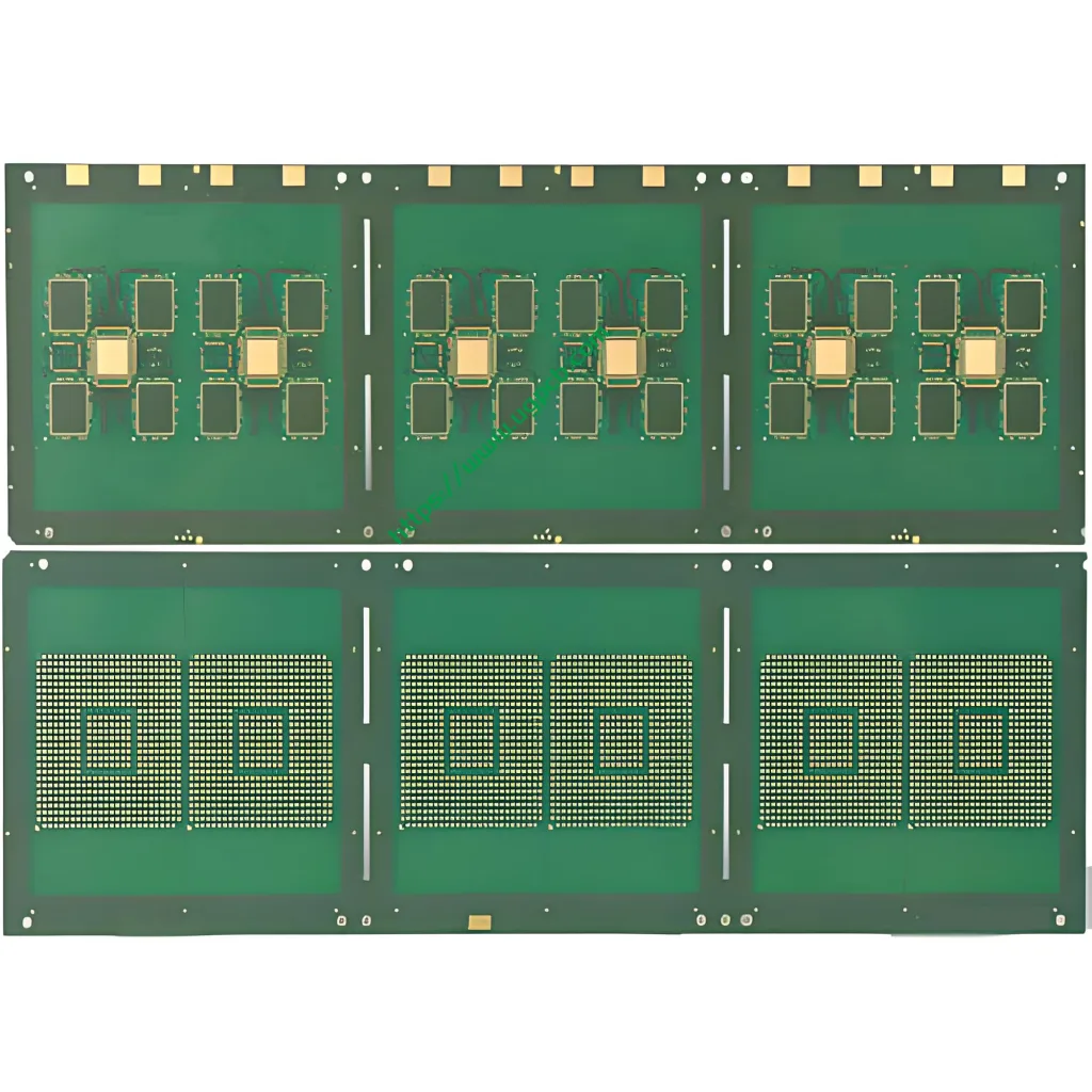
Types of Vias
Blind Vias
Buried vias only connect the via type of wiring between the inner layers, so they can’t be seen from the PCB surface.
Historical Development
From the beginning of the 20th century to the beginning of the 21st century, the PCB board industry has developed by leaps and bounds in technology, and the electronic assembly technology has been rapidly improved. As a printed PCB board industry, UGPCB can only be developed synchronously with it. With the small, light and thin electronic products, printed PCB board have developed flexible boards, rigid-flex boards, buried/blind via IC Substrate multilayer boards and so on.
Traditional Multilayer Board and the Need for Blind/Buried Vias
Speaking of blind/buried vias, first we start with the traditional multilayer board. The structure of the standard multi-layer PCB board contains inner and outer circuits, and then uses drilling and metallization processes in the holes to achieve the internal connection function of each layer of circuits. Tuttavia, because of the increase in circuit density, the packaging methods of parts are constantly updated. In order to allow the limited PCB board area to place more high-performance parts, in addition to the thinner circuit width, the diameter of the hole has also been reduced from 1 mm in the DIP jack to 0.6 mm in the SMD, and further reduced to 0.4mm and 0.3mm, Below 0.2mm. Tuttavia, it still occupies the surface area, so there will be buried vias and blind vias IC Substrate.
Increasing PCB Density with Blind and Buried Vias
The most effective way to increase PCB density is to reduce the number of through holes, and accurately set blind holes and buried holes. Blind vias IC Substrate manufacturing is very difficult. The production process of this kind of Blind vias IC Substrate board can assess the overall process level, design ability, experience and wisdom of an IC Substrate PCB factory.


