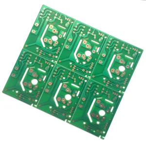
What is Bonding PCB?
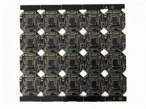
Bonding circuit board is a wiring method in chip production technology. It connects the internal circuit of the chip with gold or aluminum wire before encapsulation to the encapsulated pin or circuit board with gold-plated copper foil. Ultrasound from a 40-140kHz ultrasonic generator generates high-frequency vibration through the transducer and transmits it to a splitter by an amplitude changer. When the splitter touches the lead and soldered parts, pressure and vibration cause the metal surfaces to rub against each other, destroying the oxide film and causing plastic deformation. This results in two pure metal surfaces being closely contacted, reaching a combination of atomic distances, and creating a strong mechanical connection. The printed circuit board is usually encapsulated with black glue after bonding.
How to Identify Bonding PCB?
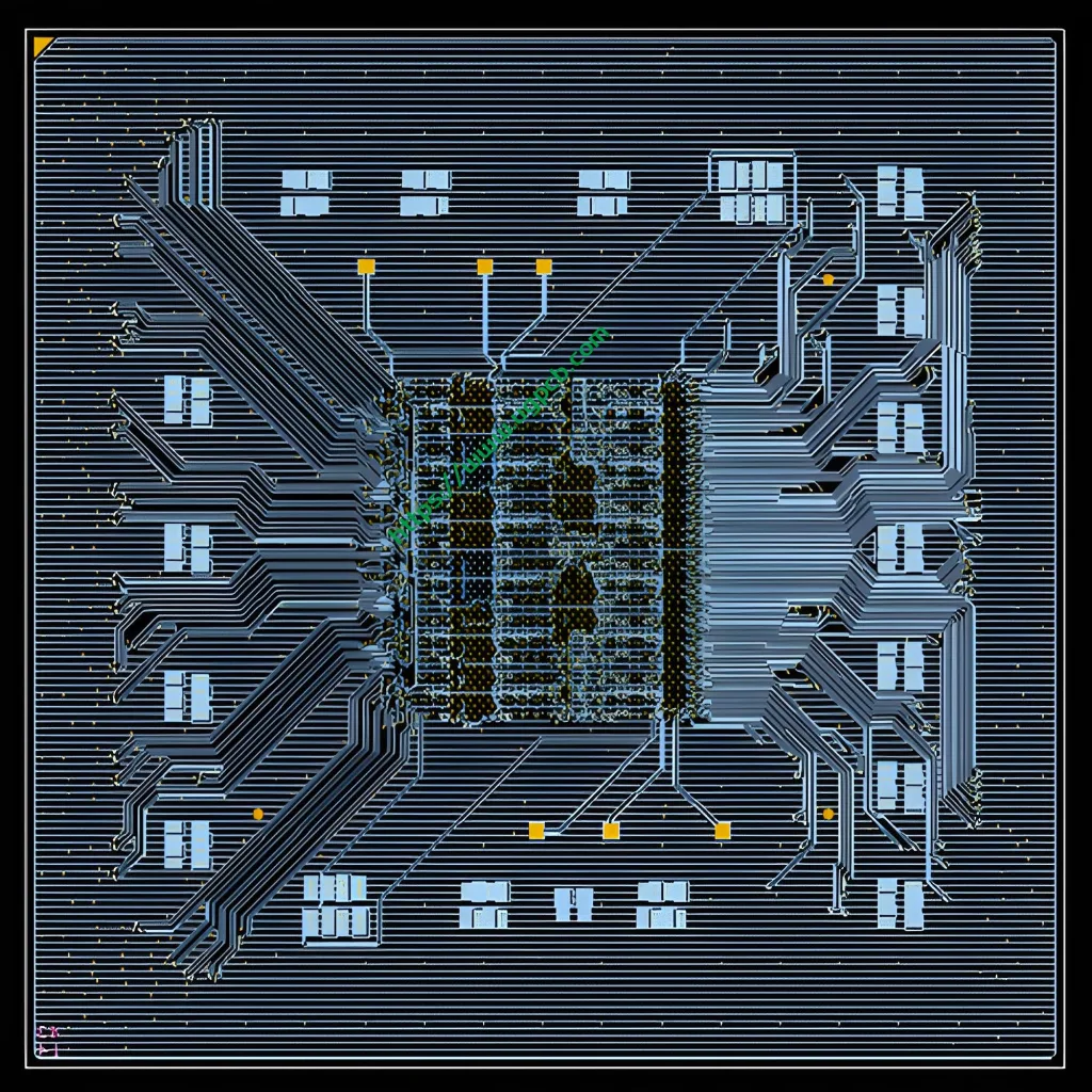
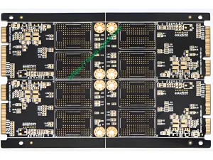
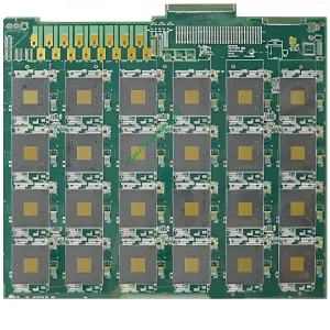
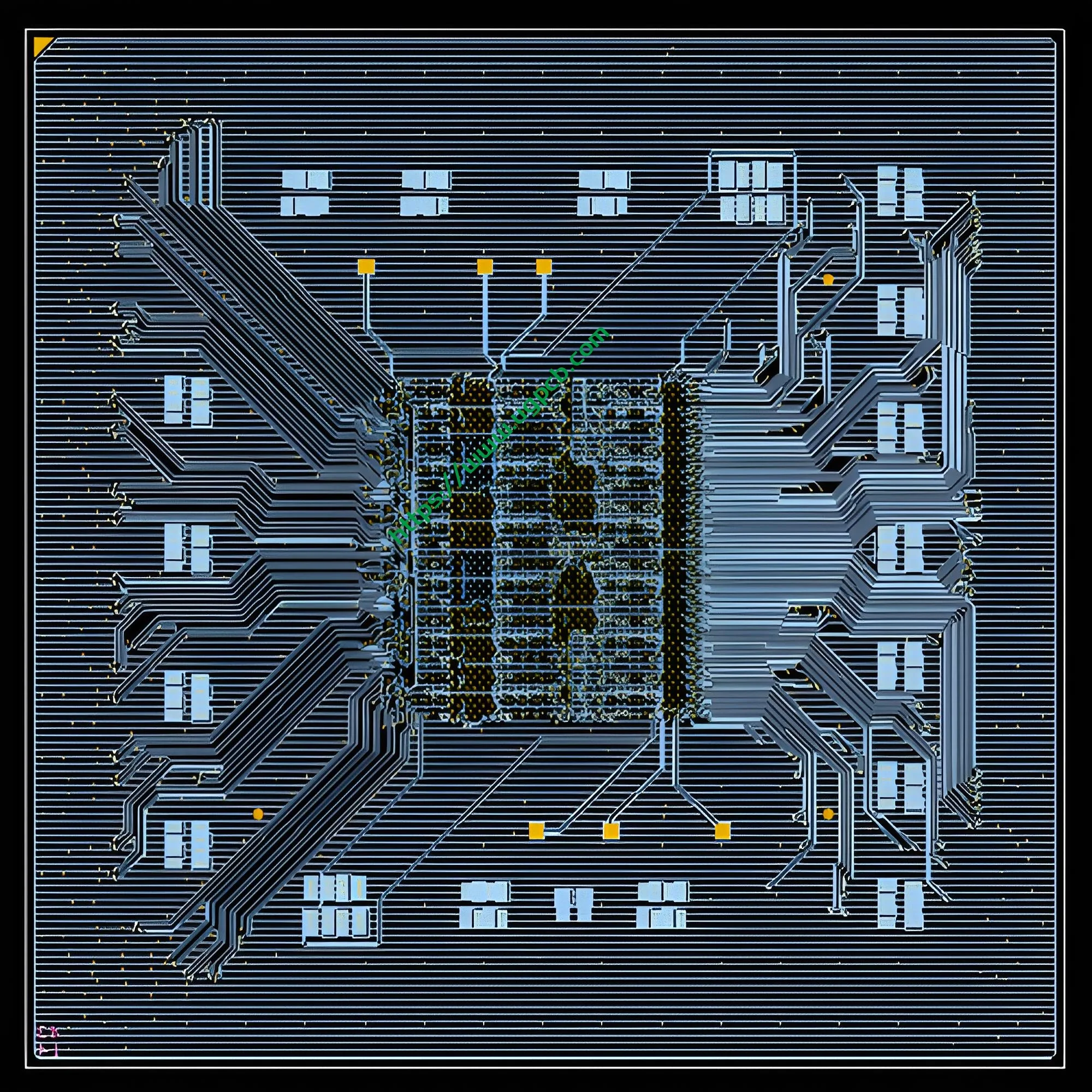
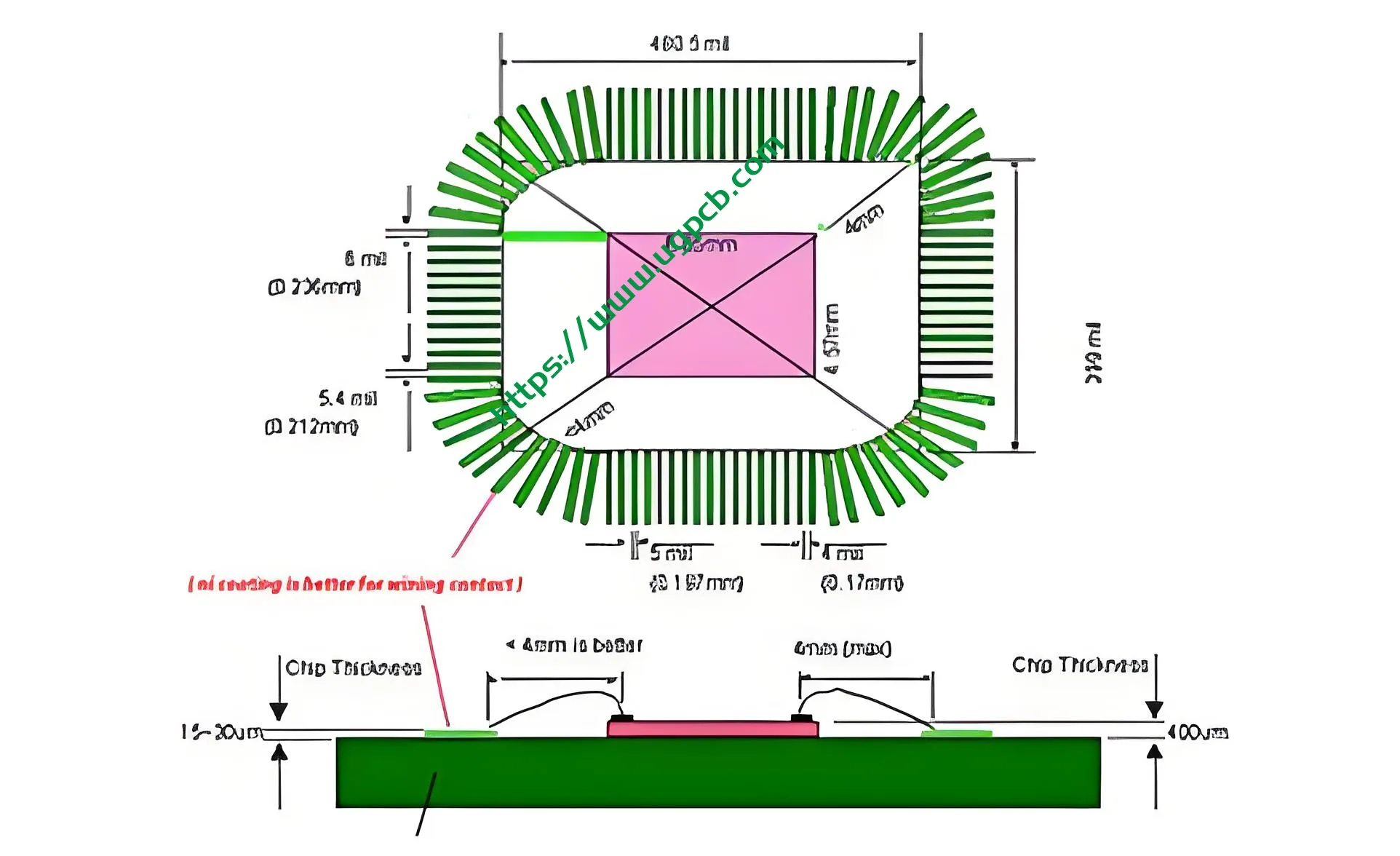
A bonding printed circuit board is a regular rectangular array, with mostly square and circular bonding pads that are thin and dense. The spacing between pads is small, and there is a regular square or circular open window pad in the middle of the bonding IC. Most bonding feet have lines leading out. The PCB state positioning acceptance standard is a (+/-) 10% bonding foot width tolerance, with a spacing requirement of more than 3mil. The bonding foot must not be disabled, and etching edges must not reduce spacing.
Advantages of Bonding Circuit Board Packaging
The bonding circuit board packaging method offers higher corrosion, shock, and stability resistance than the traditional SMT patch method. The bonding chip of the printed circuit board connects the internal circuit of the chip with the package pin of the printed circuit board through golden wires, and then precisely covers it with organic materials with special protection functions to complete the later packaging. The chip is completely protected by organic materials, isolated from the outside world, preventing humidity, static electricity, and corrosion. Allo stesso tempo, organic materials are melted at high temperature, covered on the chip, dried by the instrument, and seamlessly connected with the chip, which completely eliminates physical wear and tear and enhances stability.
PCB Bonding Process Requirements
Flusso di processo: Clean PCB – Drop Adhesive – Chip Paste – Bond – Seal – Test
- Clean PCB Circuit Board
Scrub the oil, dust, and oxide layers on the state position with a skin, then brush the test position with a brush or blow it with an air gun.
- Drop Adhesive
Medium droplets, 4 rubber points, evenly distributed in four corners. Pollution of the bonding pads is strictly prohibited.
- Chip Pasting (Crystallization)
Use a vacuum suction pen with a flat nozzle to avoid scratching the wafer surface. Check the wafer orientation and stick it to the PCB smoothly, ensuring it is parallel and there is no vacancy. The wafer and PCB should be stable and not easy to fall off during the whole process. The reserved bits of the wafer and the PCB should be positively pasted and cannot be deflected. Note that the wafer direction must not be reversed.
- State Lines
Bonding PCB should pass the bonding pull test with 1.0 lines greater than or equal to 3.5G and 1.25 lines greater than or equal to 4.5G. The standard aluminum line at the bonding melting point should have a line tail greater than or equal to 0.3 times the line diameter and less than or equal to 1.5 times the line diameter. The shape of the aluminum wire solder joint is an ellipse, with a length greater than or equal to 1.5 times the line diameter and less than or equal to 5.0 times the line diameter. The width of the solder joints should be greater than or equal to 1.2 times the line diameter and less than or equal to 3.0 times the line diameter. The state line process should be handled lightly and accurately, with operators observing the process with a microscope to detect any issues such as breaking state, winding line, offset, hot and cold welding, or starting aluminum. Any issues should be reported to relevant technical personnel for timely resolution. Before formal production, a first inspection by a special person is required to check for state errors such as Shaobang or Leaky State. Durante la produzione, a special person should regularly check its correctness (up to every 2 ore).
- Sealing
Before sealing, check the plastic ring’s regularity and ensure its center is square and without visible distortion. During installation, ensure the bottom of the plastic ring fits closely with the wafer surface and that the light-sensitive area in the center is not blocked. When dispensing, the black glue should completely cover the aluminum wire of the PCB solar circle and the bonding wafer, with no rubbing. The black glue cannot seal out the PCB solar circle, and any glue leakage should be erased in time. The black glue cannot penetrate the wafer through the plastic ring. During the gel dripping process, avoid touching the wafer surface and the bonded wires inside the plastic ring with pins or hair picks. The drying temperature is strictly controlled: the preheating temperature is 120 +5 degrees Celsius for 1.5-3.0 minuti, and the drying temperature is 140 +5 degrees Celsius for 40-60 minuti. The dry black rubber surface must not have air holes, and it should not have a cured appearance. The black rubber height must not be higher than the plastic ring.
- Bonding PCB Testing
Combine multiple testing methods:
UN. Artificial Visual Detection
B. Automatic wire quality detection for the bonding machine
C. Automatic Optical Image Analysis (AOI) X-ray analysis to check the quality of inner solder joints
 LOGO UGPCB

