
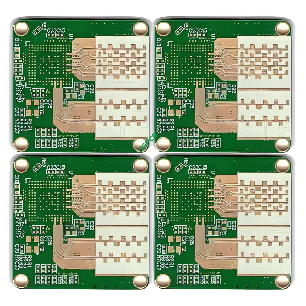
Overview of High Frequency PCB
A high-frequency PCB is a specialized type of circuit board designed to operate at high frequencies, typically in the range of gigahertz (GHz). These PCBs are essential for applications that require precise signal transmission and minimal signal loss. They are widely used in industries such as telecommunications, sistemi radar, and satellite communications. The quality standard for high-frequency PCBs is IPC 6012 Class 2, ensuring high reliability and performance.
Definition and Key Specifications
A high-frequency PCB is defined by its ability to handle signals at very high frequencies while maintaining signal integrity. La costante dielettrica (dk) of these PCBs ranges from 2.0 A 1.6, which is crucial for controlling signal speed and impedance. The number of layers can vary from 1 A 36, providing flexibility for different design requirements. The thickness of the PCB ranges from 0.254mm to 12mm, and the copper thickness can be either 0.5oz or 1oz. Surface technologies include Silver, Oro, and OSP, each offering different benefits in terms of solderability and corrosion resistance. Special processes like mixed materials and stepped grooves further enhance the performance of high-frequency PCBs.
Design Considerations
When designing a high-frequency PCB, several factors must be considered:
- Costante dielettrica (dk): The dk value between 2.0 E 1.6 is critical for maintaining signal integrity at high frequencies.
- Number of Layers: The wide range of layer options (1 A 36) allows for customization based on specific application needs.
- Spessore: The thickness range from 0.254mm to 12mm provides flexibility in design, catering to different spatial and functional requirements.
- Spessore del rame: The choice between 0.5oz and 1oz base copper affects the current-carrying capacity and signal integrity.
- Surface Technology: Options like Silver, Oro, and OSP provide different levels of solderability and corrosion resistance.
- Special Processes: Techniques like mixed materials and stepped grooves can significantly enhance the performance of high-frequency PCBs.
Principio di lavoro
High-frequency PCBs operate based on the principle of controlled impedance and minimal signal loss. The dielectric constant of the materials used ensures that signals travel with minimal delay and loss, maintaining their integrity. The precise control over thickness and copper weight allows for consistent impedance, which is critical for high-frequency signal transmission. Surface technologies like Silver, Oro, and OSP provide reliable connection points for components, ensuring efficient signal transfer.
Applicazioni
High-frequency PCBs are used in a variety of applications that require high-speed data transmission and signal integrity:
- Telecommunications: Ensuring clear and reliable signal transmission in mobile phones, base stations, and other communication devices.
- Radar Systems: Providing accurate and reliable signal processing in military and civilian radar systems.
- Satellite Communications: Facilitating rapid and reliable data transfer between ground stations and satellites.
Classificazione
High-frequency PCBs can be classified based on several criteria:
- Frequency Range: Typically operating at gigahertz (GHz) frequencies.
- Number of Layers: Ranging from 1 A 36 strati, depending on the complexity of the circuit.
- Spessore: Options from 0.254mm to 12mm allow for customization based on specific application needs.
- Spessore del rame: Standard and heavy copper options (0.5oz and 1oz) cater to different current-carrying capacities.
- Surface Technology: Choices like Silver, Oro, and OSP provide different levels of solderability and corrosion resistance.
Material Properties
The key properties of high-frequency PCB materials include:
- Low Dielectric Constant: Ensures minimal signal delay and loss, making them suitable for high-frequency applications.
- Wide Thickness Range: Allows for flexibility in design, catering to different spatial and functional requirements.
- Excellent Signal Integrity: Maintains signal integrity even at high frequencies, ensuring reliable performance.
- Reliable Connection Points: Surface technologies like Silver, Oro, and OSP provide strong and reliable connection points for components.
Processo di produzione
The production of a high-frequency PCB involves several steps:
- Material Selection: Choosing materials with a low dielectric constant and high signal fidelity.
- Circuit Design: Creating the circuit layout with considerations for high-frequency performance and signal integrity.
- Incisione: Removing unnecessary copper to create the desired circuit pattern.
- Lamination: Bonding multiple layers together under high pressure and temperature to ensure a strong and reliable connection.
- Surface Finishing: Applying surface technologies like Silver, Oro, or OSP to enhance solderability and corrosion resistance.
- Special Processes: Utilizing techniques like mixed materials and stepped grooves to further enhance performance.
- Testing and Quality Control: Ensuring the final product meets all specifications and standards.
Use Scenarios
High-frequency PCBs are used in scenarios where high-speed data transmission and signal integrity are critical:
- Mobile Phones: Ensuring clear and reliable signal transmission in modern smartphones.
- Base Stations: Providing accurate and reliable signal processing in communication infrastructure.
- Radar Systems: Enabling precise and reliable signal processing in military and civilian radar applications.
- Satellite Communications: Facilitating rapid and reliable data transfer between ground stations and satellites.
In sintesi, high-frequency PCBs are specialized circuit boards designed for high-speed data transmission and signal integrity. Their low dielectric constant, wide thickness range, and excellent signal fidelity make them ideal for applications in telecommunications, sistemi radar, and satellite communications.


