
Materiale
The Step slot PCB board is manufactured using FR-4 TG170 material. FR-4 stands for Flame Retardant 4, a grade of epoxy resin-based laminate that is widely used in the production of printed circuit boards (PCB) due to its excellent electrical properties, resistenza meccanica, e resistenza al calore. The TG170 indicates a glass transition temperature of 170°C, ensuring the board maintains its structural integrity and electrical performance even under high-temperature conditions.

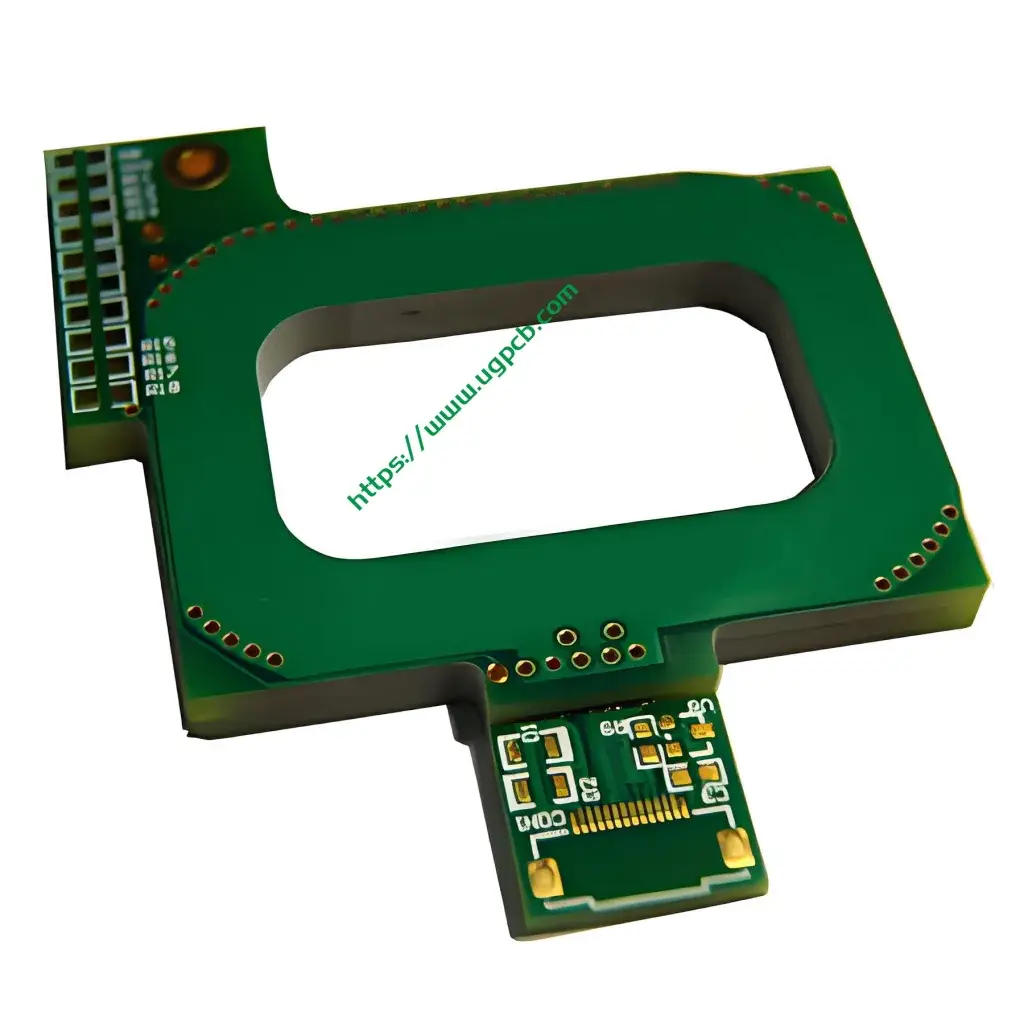
Prestazione
This PCB board features a 4-layer design, which allows for more complex circuitry and higher component density. The copper thickness of 1OZ (ounce per square foot, approximately 35 microns) provides good conductivity and current carrying capacity. With a finished thickness of 2.0mm, the board offers robust physical durability. The immersion gold surface treatment enhances the solderability of the board, reducing the risk of corrosion and improving reliability in electronic assemblies.
Caratteristiche
The Step slot PCB board is distinguished by its unique step slot design. This special process creates a stepped or tiered opening in the board, allowing for more flexible routing of traces and components, especially in compact designs. The trace/space of 6mil/6mil (0.152mm/0.152mm) ensures precise and reliable electrical connections, while the minimum hole size of 0.3mm (12mil) facilitates the use of small components and tight packaging.
Flusso di produzione
The production of Step slot PCB boards involves several critical steps:
- Material Preparation: FR-4 TG170 laminate is cut to size and prepared for processing.
- Copper Lamination: Thin sheets of copper are bonded to the laminate to form the conductive layers.
- Perforazione: Precision drilling creates the vias and component holes, including the special step slot features.
- Plating: The holes are plated with copper and, subsequently, immersion gold to prepare them for soldering.
- Circuit Patterning: Using photolithography, the copper is etched away to form the desired circuit patterns.
- Soldermask Application: A protective layer of soldermask is applied to protect the circuitry and provide a smooth surface for component placement.
- Surface Finish: The immersion gold treatment is applied to enhance solderability.
- Final Inspection and Testing: Each board undergoes rigorous inspection and testing to ensure it meets quality standards.
Application Scenarios
The Step slot PCB board is ideally suited for use in module PCB boards. Its compact design, high component density, and enhanced electrical performance make it an excellent choice for applications requiring intricate circuitry and reliable performance. Examples include:
- Apparecchiature per le telecomunicazioni: High-density interconnect modules for signal processing and transmission.
- Computer Hardware: Motherboards, schede grafiche, and other components requiring complex circuitry.
- Industrial Automation: Control systems and sensors that require reliable and compact PCB solutions.
- Elettronica di consumo: Smartphones, compresse, and other devices where space is a premium and high performance is essential.
In sintesi, the Step slot PCB board combines advanced materials, precise manufacturing processes, and unique design features to meet the demands of high-performance electronic applications.


