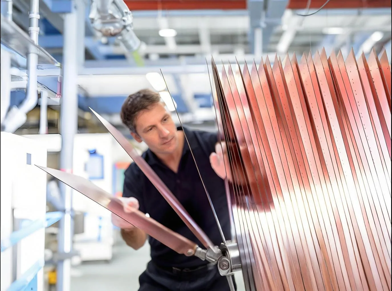
F4BME-2-A TEFLON PCB in tessuto in vetro laminati rivestiti di rame
F4BME-2-A TEFLON PCB in tessuto in vetro Laminati rivestiti di rame sono fabbricati utilizzando tessuto in tessuto importato, Resina PCB Teflon, e riempitivo con una membrana nano-ceramica. Questo prodotto aderisce a formulazioni scientifiche e rigorosi processi tecnologici, Utilizzo del foglio di rame a bassa rugosità. Supera la serie F4BM in prestazioni elettriche e stabilità della resistenza all'isolamento superficiale, Vantando un indice di intermodulazione più elevato rispetto a F4BME-1/2.
Specifiche tecniche
Aspetto: Soddisfa i requisiti di specifica per i laminati PCB a microonde secondo gli standard nazionali e militari.
Tipi:
- F4BME-2-A255
- F4BME-2-A262
- F4BME-2-A275
- F4BME-2-A285
- F4BME-2-A294
- F4BME-2-A300
Dimensioni (mm):
- 550*440
- 500*500
- 600*500
- 650*500
- 1000*850
- 1100*1000
- 1220*1000
- 1500*1000
Le dimensioni personalizzate sono disponibili su richiesta.
Spessore e tolleranza (mm):
| Spessore laminato | Tolleranza |
|---|---|
| 0.254 | ± 0,025 |
| 0.508 | ± 0,05 |
| 0.762 | ± 0,05 |
| 0.787 | ± 0,05 |
| 1.016 | ± 0,05 |
| 1.27 | ± 0,05 |
| 1.524 | ± 0,05 |
| 2.0 | ± 0,075 |
| 3.0 | ± 0,09 |
| 4.0 | ± 0,1 |
| 5.0 | ± 0,1 |
| 6.0 | ± 0,12 |
| 9.0 | ± 0,18 |
| 10.0 | ± 0,18 |
| 12.0 | ± 0,2 |
Resistenza meccanica:
- Taglio/punzonatura:
- Spessore <1mm: Nessun bara dopo il taglio; Lo spazio minimo tra due fori di punzonatura è 0,55 mm, Nessuna delaminazione.
- Spessore >1mm: Nessun bara dopo il taglio; Lo spazio minimo tra due fori di punzonatura è 1,10 mm, Nessuna delaminazione.
- Forza della pelatura (1once di rame):
- Stato normale: ≥14n/cm; Nessuna bolla o delaminazione della forza della buccia: ≥12n/cm (sotto costante umidità e temperatura, mantenuto in saldatura a fusione a 265 ° C ± 2 ° C per 20 secondi).
Proprietà chimica: Il metodo di incisione chimica per PCB può essere utilizzato senza alterare le proprietà dielettriche del laminato. La placcatura attraverso i fori richiede un trattamento con sodio o un trattamento al plasma.
Proprietà elettrica:
| Nome | Condizione di prova | Unità | Valore |
|---|---|---|---|
| Densità | Stato normale | g/cm³ | 2.1~ 2.35 |
| Assorbimento di umidità | Immergere in acqua distillata a 20 ± 2 ° C per 24 ore | % | ≤0,07 |
| Temperatura operativa | Camera di temperatura ad alta bassa | ° C. | -50° C ~+260 ° C. |
| Conducibilità termica | W/m/k | 0.45~ 0,55 | |
| Cte (tipico) | -55~ 288 ° C. (εr :2.5~ 2.9) | ppm/° C. | X: 16, Y: 20, Z: 170 |
| Cte (tipico) | -55~ 288 ° C. (εr :2.9~ 3.0) | ppm/° C. | X: 12 Y: 15 Z: 90 |
| Fattore di restringimento | 2 ore in acqua bollente | % | <0.0002 |
| Resistività superficiale | DC, 500V, Stato normale | Mω | ≥4*10^5 |
| Resistività al volume | Stato normale | Mω · cm | ≥6*10^6 |
| Resistenza dielettrica superficiale | d = 1mm(Kv/mm) | ≥1.2 | |
| Costante dielettrica | 10GHz | Vedi la tabella sotto | |
| Fattore di dissipazione | 10GHz | Vedi la tabella sotto | |
| Pimd (2.5GHz) | db | -160 |
Classificazione di infiammabilità UL: 94 V-0
Per ulteriori informazioni o per effettuare un ordine, Visita il nostro sito Web www.ugpcb.com o contattaci via e -mail all'indirizzo sales@ipcb.com.
Prodotti UGPCB:
UGPCB offre una vasta gamma di prodotti tra cui:
- Radio/microonde/ibrido ad alta frequenza FR4 Double/Multiyer 1 ~ 3+N+3 HDI, Anylayer HDI, Rigido-flesso, Blind Buried Slot, Board di rame pesante IC con traino, e altro.
In caso di domande o hai bisogno di ulteriore assistenza, Non esitare a contattarci tramite il nostro sito Web o a inviare una richiesta direttamente a sales@ugpcb.com.
