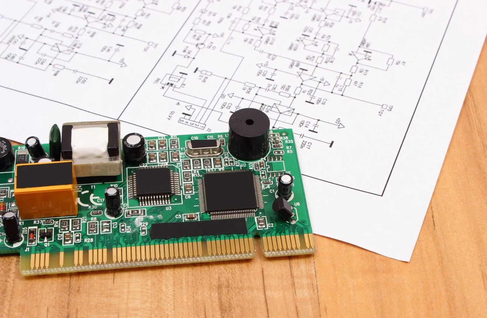
多層 PCB 設計
多層 PCB 設計: Experts in Precision Interconnection Architecture for High-Reliability Complex Systems
In the era of high-speed digital and mixed signals, multilayer PCB design has become the core carrier for high-end electronic systems such as communication base stations, 産業用制御, and medical equipment. We specialize in the design and manufacturing of 12-48 layer high-complexity PCBs, providing global customers with full-cycle solutions from prototype verification to mass delivery through scientific interlayer planning, precise electromagnetic compatibility control, and innovative thermal synergy design.
Core Technology Advantages
High-Density Interconnection Architecture Design
- Supports 3 + N + 3 to Any-layer HDI stacking, with blind and buried hole accuracy of ±50μm, achieving 20μm micro-via interconnection and increasing wiring density by 60%.
- Employs dynamic phase compensation technology to ensure the insertion loss of 56Gbps high-speed signals is less than 0.5dB/inch, meeting the IEEE 802.3bj standard.
Mixed Signal Integrity Assurance
- Optimizes power ground plane segmentation (plane resonance suppression > 30dB) through ANSYS HFSS/PI collaborative simulation.
- Customized impedance control scheme (tolerance ±5%) supports DDR5/PCIe 6.0 protocol impedance matching requirements.
Thermal Coupling Optimization Design
- Develops a gradient thermal conductivity hole matrix based on thermal simulation (FloTHERM) and actual measurement data, reducing thermal resistance by 40%.
- Supports metal core/ceramic composite structure, suitable for high power density scenarios over 100W/cm².
Process Manufacturing Barriers
Precision Lamination Technology
- Uses a vacuum lamination system (registration accuracy ±25μm), combined with low CTE materials (<14ppm/℃), to solve the warping problem of boards with more than 32 レイヤー.
Special Material Application
- Provides high-frequency plates such as Megtron 6 and FR – 4 HT (Dk = 3.7±0.05@10GHz), supporting extreme environments from -55℃ to 260℃.
Detection System
- 100% implementation of TDR testing (resolution 5ps) and 3D X-ray hole copper detection (thickness tolerance ±8μm).
Industry Solutions
5G Base Station
- Designs 28-layer hybrid pressure PCB, realizing the collaborative optimization of radio frequency, digital, and power modules, with insertion loss reduced by 25%.
航空宇宙
- Passes MIL – PRF – 31032 認証, improving the vibration resistance performance of 32-layer backplane by 50%.
カーエレクトロニクス
- Develops 16-layer arbitrary order HDI, integrating 12μm ultra-fine lines, passing AEC – Q100 temperature cycle test.
Full Link Promise from Design to Delivery
DFM Expert System
- Based on a library of over 2000 successful cases, predicting and avoiding 90% of manufacturability risks.
Rapid Response Mechanism
- Completes the design review of 16-layer boards within 72 時間, supporting customization of 1 – 12oz copper thickness.
Zero Defect Delivery
- Executes IPC – あ – 600 クラス 3 standard to ensure a first pass rate of over 99.95%.
Explore More
Schedule a consultation with a technical advisor to start your journey of innovation in precision electronic systems!
Define performance with stacking and carry the future with precision. We make every circuit layer a cornerstone of reliability.
 UGPCBのロゴ
微信
WeChat で QR コードをスキャンします