
18layers通信基地局PCBの紹介
The 18Layers Communication Base Station PCB is a sophisticated and high-performance printed circuit board designed specifically for use in communication base stations. This PCB offers exceptional durability, 信頼性, and efficiency, making it an ideal choice for critical communication infrastructure applications.
Key Features and Specifications
材料
- 材料: The PCB is made from Panasonic M6, a high-quality material known for its excellent electrical properties and thermal stability. This ensures that the PCB can withstand harsh environmental conditions and maintain optimal performance.
Layers and Copper Thickness
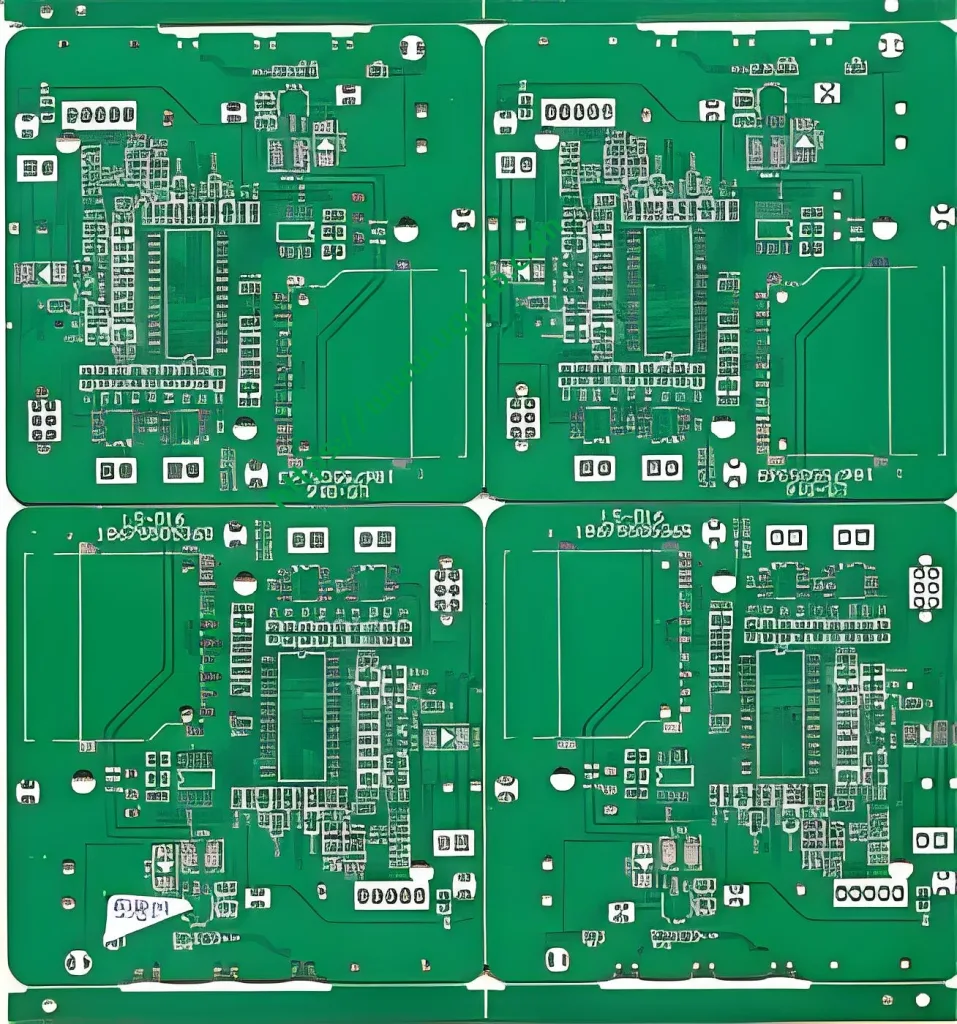
- レイヤー: と 18 レイヤー, this PCB provides extensive space for complex circuit designs required in advanced communication systems.
- 銅の厚さ: The copper thickness ranges from 0.5 に 1 オンス, allowing for robust signal transmission and power distribution across the board.
Dimensions and Surface Treatment
- 仕上がり厚さ: The PCB has a finished thickness of 2.0mm, which provides structural integrity and mechanical strength.
- 表面処理: It features an immersion gold surface treatment. This not only enhances the aesthetic appeal but also improves solderability, 耐食性, and contact reliability.
Precision Design
- Trace/Space: Featuring precise trace/space measurements of 4mil/4mil (0.1MM/0.1MM), this PCB ensures high-density interconnectivity with minimal crosstalk and signal loss.
- ミンホール: The minimum hole size is 0.2mm (8ミル), enabling fine-pitch components and high-density layouts.
特別なプロセス
- 特殊加工: The PCB incorporates a metal edging process, which adds extra strength and protection to the edges, enhancing the overall durability and lifespan of the board.
アプリケーション
The 18Layers Communication Base Station PCB is primarily used in communication base station applications where high reliability and performance are crucial. これらには含まれます:
- Mobile network base stations
- Radio frequency (RF) transceivers
- Microwave communication systems
- Data center networking devices
製造工程
The manufacturing process of the 18Layers Communication Base Station PCB involves several meticulous steps to ensure the highest quality standards:
- 材料の選択: High-grade Panasonic M6 material is selected for its superior electrical properties and durability.
- レイヤースタッキング: The 18 layers are carefully stacked and bonded together using advanced laminating techniques.
- Etching and Drilling: Precision etching and drilling processes create the intricate circuit patterns and holes necessary for component placement.
- Plating and Soldermask Application: 浸漬ゴールドメッキとセルダーマスクアプリケーションは最終的な表面処理を提供します, 優れた導電性と環境要因に対する保護を確保する.
- 品質管理: 各PCBは、出荷のためにパッケージ化される前に厳しい品質基準を満たすために厳しいテストと検査を受けます.
結論
18layers通信基地局PCBは、最新のコミュニケーションインフラストラクチャの厳しい要件を満たすために設計された高度に専門化された製品です。. その高度な材料, 精密設計, そして、厳しい製造プロセスは、あらゆる高性能通信システムに信頼できる選択肢となります. モバイルネットワークベースステーションを構築しているか、データセンター機器を建設しているか, このPCBは、比類のない信頼性とパフォーマンスを提供します.


