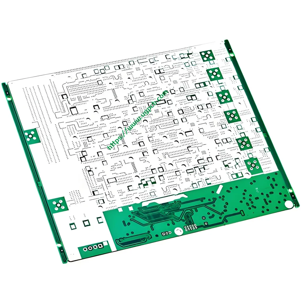
プリント基板設計, PCB製造, プリント基板, PECVD, ワンストップサービスを使用したコンポーネントの選択

ダウンロード | について | 接触 | サイトマップ

4-層ロジャース スプレー錫 PCB ボード - UGPCB

高周波プリント基板/

4-層ロジャース スプレー錫 PCB ボード

名前: 4-層ロジャース スプレー錫 PCB ボード

皿: Rogers4350B

レイヤー: 4L

板厚: 1.6mm

Outer copper thickness: 2 オズ

Inner copper thickness: 1 オズ

Minimum hole diameter: 0.3mm

最小ライン幅/線間隔: 5ミル

表面処理: spray tin

Product use: base station sub board

Process difficulty: 鉛フリースプレースズ

  • 製品詳細

Composition and Structure

4-layer PCB means that the printed circuit board is made of 4 layers of fiberglass. There are four routing layers: top, bottom, VCC, and GND. 一般的に, 穴を通して, buried holes, and blind holes are used to connect the layers. There are more buried and blind vias than double-sided.

設計上の考慮事項

加えて, try not to run signal traces on the VCC and GND layers.

Advantages Over Double-sided Rogers PCB Boards

Compact Design

4-layer PCB boards have many advantages over double-sided Rogers PCB boards. They can be designed to be more compact.

Improved Noise Immunity

They have significantly improved noise immunity.

Easier Layout

And are easier to lay out.

前へ:

次:

返信を残す

伝言を残す