Structure and Composition
Base Plate and Layers
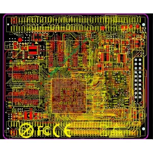
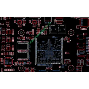
The high-frequency hybrid splint includes a base plate, which is folded and positioned on the first inner wire layer, the first outer wire layer, and the top surface of the solder mask ink layer from bottom to top. The second layer of the solder resist ink layer is also present.
Substrate Divisions
The substrate includes a high-frequency area and an auxiliary area. The auxiliary area is fixed, and the inlay in the high-frequency area should be located at a fixed position.
Utility Model and Design
Division of Splint
The utility model provides a high-frequency hybrid splint, which is divided into two parts: a high-frequency area and an auxiliary area. It provides mechanical support.
High-Frequency Area Arrangement
The high-frequency area is independently arranged, and only the high-frequency area is made of high-frequency materials. This minimizes the use of high-frequency board materials and reduces production costs while satisfying high-frequency signals.
Product Specifications
Classification and Layers
- High Frequency Hybrid Product Classification Layers: 6 レイヤー
Board Material and Thickness
- Used Board: ロ4350b + FR4
- 厚さ: 1.6mm
Size and Surface Treatment
- サイズ: 210mm*280mm
- 表面処理: Gold-plated
Minimum Aperture and Application
- Minimum Aperture: 0.25mm
- 応用: コミュニケーション
特徴
- High Frequency Mixed Pressure
 UGPCBのロゴ
