材料構成
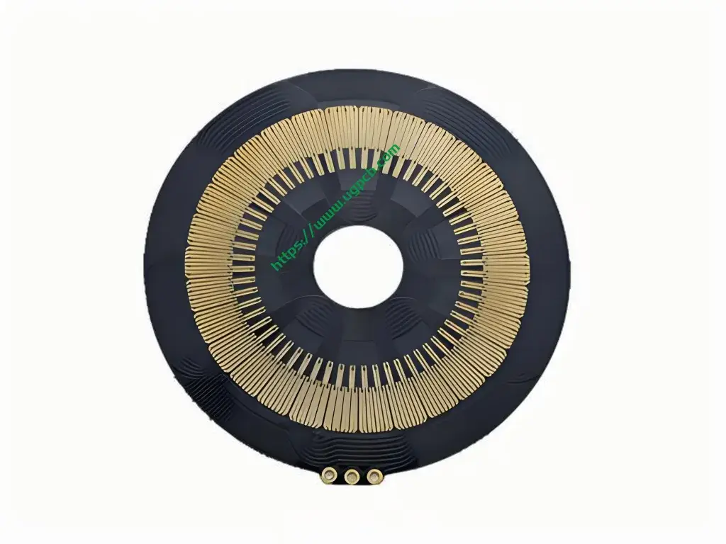
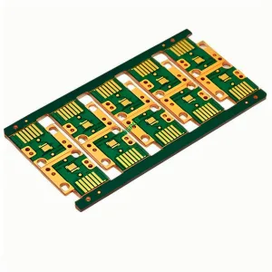
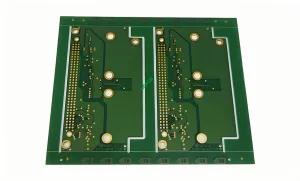
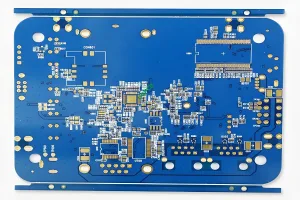
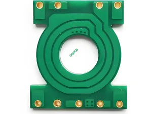
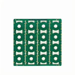
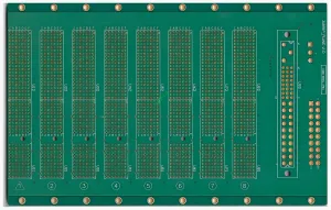
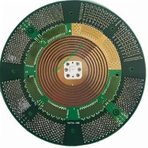
The Carbon Film Hybrid Integrated PCB is crafted from a unique blend of materials that ensure its robustness and functionality. It features a Ceramic Substrate as its foundational layer, providing exceptional thermal stability and mechanical strength. This substrate is then combined with Carbon oil, enhancing its electrical conductivity and durability.
性能特性
This PCB stands out due to its impressive performance specifications. With a PCB thickness of 0.6mm, it offers a balance between rigidity and flexibility. The Copper Thickness of 1OZ (351つ) ensures efficient heat dissipation and excellent current carrying capacity. The Line width of 0.2mm and Minimum aperture of 0.3mm facilitate intricate circuit designs and precise component placement, それぞれ.
特徴的な機能
The gold-plated surface treatment not only enhances the aesthetic appeal of the PCB but also provides superior corrosion resistance and electrical conductivity. The 2-Layer design allows for more complex circuitry while maintaining compact dimensions, making it ideal for applications requiring high density and integration.
製造工程
The production of Carbon Film Hybrid Integrated PCB involves several meticulous steps. Initially, the Ceramic Substrate is prepared and coated with Carbon oil to form the conductive layer. Precision etching techniques are then employed to create the intricate circuit patterns according to the specified Line width and aperture dimensions. Following this, the copper foil is laminated to the substrate, achieving the desired Copper Thickness. The final step involves gold-plating the surface for enhanced durability and conductivity, resulting in a finished PCB of 0.6mm thickness.
アプリケーションシナリオ
The versatility of Carbon Film Hybrid Integrated PCB makes it an excellent choice for a wide range of applications. In the computer industry, it supports high-speed data processing and efficient heat management. Within the automobile sector, it ensures reliable performance in electronic control units and sensors. It is also widely used in communication devices for signal integrity and stability. Instrumentation and power supply systems benefit from its compact design and robust electrical properties, making it a valuable component in various industries.
 UGPCBのロゴ

