そして,プリント基板, PCBA および PECVD のカスタマイズ, 試作・製造プロデューサー

ダウンロード | について | 接触 | サイトマップ

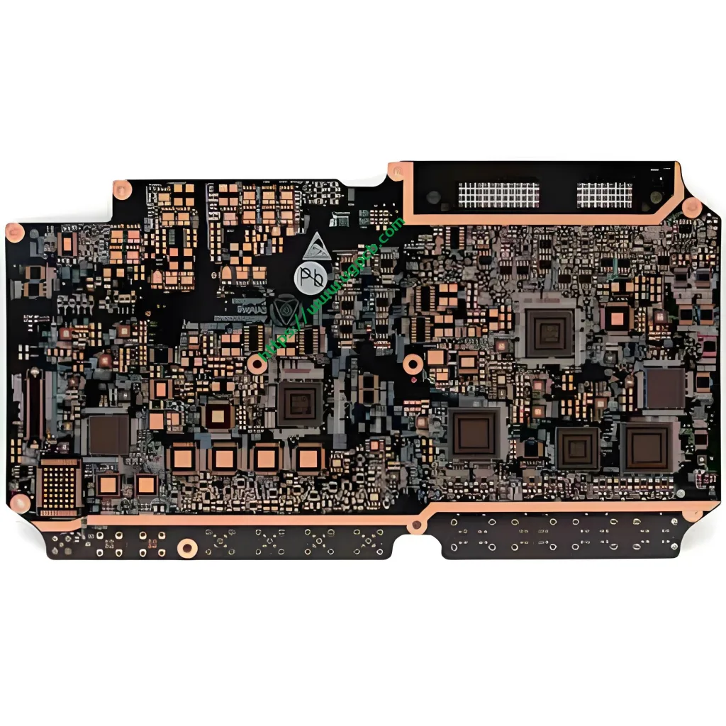
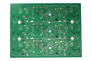
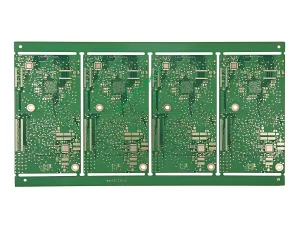
通信機器 2+N+2 HDI PCB ボード - そして

HDI PCB/

通信機器 2+N+2 HDI PCB ボード

名前: Automotive communication 2+N+2 HDI board

Plate: S1000-2M

レイヤー: 14L

材料: イソラ

Plate thickness: 1.6±0.16mm

Minimum aperture laser hole: 0.10mm

Mechanical hole: 0.20mm

Minimum track/spacing: 75/751つ

Minimum plate thickness and porosity: 8:1

特殊加工: 2 laser drilling, 3 押す, 2+N+2 HDI board

Use: vehicle communication

  • 製品詳細

製造工程

Material and Surface Treatment

The second-order HDI board for automotive communication is manufactured using Shengyi S1000-2M material, which undergoes immersion gold surface treatment.

レーザー穴あけ加工

Laser drilling is one of the processes employed in the manufacturing of this circuit board.

応用

Automotive Communications

The circuit board is widely used in the field of automotive communications.

前へ:

次:

返信を残す

伝言を残す