
Introduction to Fibre-Optical Module PCB
Overview and Definition
Fibre-Optical Module PCBs, also known as Fiber Optic Boards, are specialized printed circuit boards (プリント基板) designed for use in fiber optic communication systems. These PCBs are integral components in modern telecommunications and data transmission networks due to their ability to handle high-speed data transfer with minimal signal loss.
目的とアプリケーション
The primary purpose of a Fibre-Optical Module PCB is to provide a reliable platform for mounting and interconnecting optical components such as lasers, photodetectors, and other optoelectronic devices. These PCBs are commonly used in:
- Telecommunications equipment
- Data centers
- High-speed networking devices
- 医用画像機器
- Industrial automation systems
分類
Fibre-Optical Module PCBs can be classified based on several criteria including:
- レイヤー数 (例えば。, single-layer, 両面, 多層)
- Material composition (例えば。, 私を玉座にしてください 6, Panasonic M6)
- インピーダンス制御 (例えば。, 50 オーム, 100 オーム)
- 表面処理 (例えば。, 浸漬ゴールド, gold fingers)
Material and Build
材料
The Fibre-Optical Module PCB utilizes MEGTRON 6, also known as Panasonic M6, which is a high-performance material offering excellent thermal stability and mechanical strength. This makes it ideal for applications requiring durability and reliability.
建設の詳細
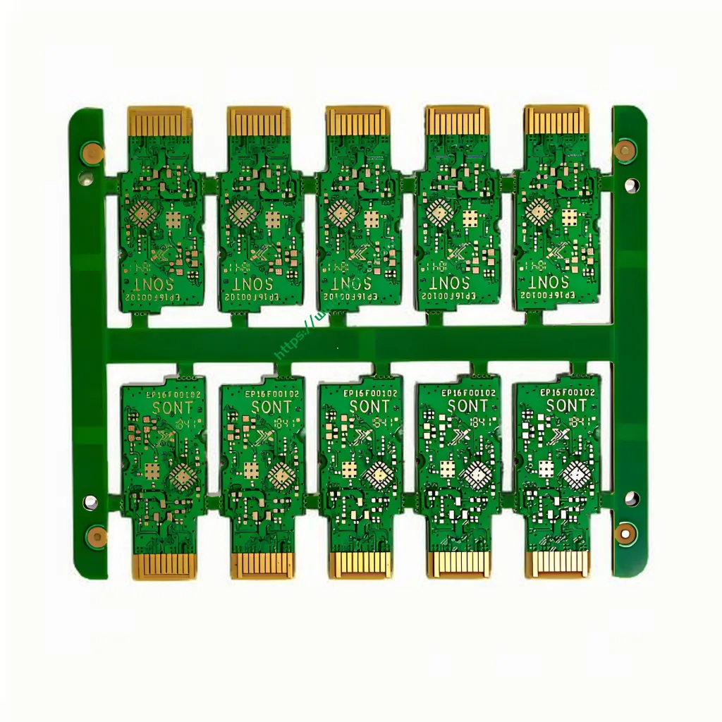
- レイヤー: PCBは構成されています 8 レイヤー, providing ample space for complex circuit designs and component placement.
- 色: 緑と白で利用可能, allowing for easy differentiation and identification in various applications.
- 仕上がり厚さ: The PCB has a finished thickness of 1.0mm, optimizing both structural integrity and space efficiency.
- 銅の厚さ: With a copper thickness of 1OZ (ounce), PCBは、効率的な電気伝導率を保証します.
性能特性
- Impedance Control: The PCB maintains impedance values of 100 ± 7% そして 50 ± 10%, ensuring consistent signal transmission quality.
- Speed: Capable of handling speeds up to 400g, 高周波アプリケーションに適しています.
- 許容範囲: The tolerance between the gold finger and plate edge is ±0.05mm, ensuring precise alignment and connection reliability.
製造工程
The manufacturing process of a Fibre-Optical Module PCB involves multiple stages including:
- 材料の準備: Selecting and preparing the base material (私を玉座にしてください 6).
- レイヤースタッキング: Stacking multiple layers of the PCB material to achieve the desired thickness and functionality.
- パターンエッチング: Using chemical etching or laser cutting to create the circuit patterns on each layer.
- ラミネート加工: 高圧と温度の下で層を一緒に圧縮して凝集ユニットを形成する.
- メッキ: Applying copper plating to the PCB surface to ensure good electrical connectivity.
- 表面処理: Treating the surface with immersion gold and adding gold fingers to improve conductivity and corrosion resistance.
- 品質管理: PCBがすべてのパフォーマンス仕様を満たすことを確認するために厳格なテストを実施する.
主な機能と利点
- High Signal Integrity: Maintains signal purity over long distances, crucial for fiber optic communications.
- 耐久性: Made from robust materials that withstand harsh environmental conditions.
- Precision: High precision in manufacturing ensures reliable connections and minimal signal loss.
- 多用途性: Suitable for a wide range of applications due to its adaptable design and material properties.
使用シナリオ
Fibre-Optical Module PCBs are essential in scenarios where high-speed data transmission is critical, のような:
- Telecommunication Networks: Ensuring seamless data flow across vast distances.
- Data Centers: Supporting the backbone of data storage and retrieval operations.
- 医療機器: Enhancing the performance of diagnostic and imaging devices.
- 産業用アプリケーション: Facilitating automation and control systems with high precision and reliability.
結論は, the Fibre-Optical Module PCB represents a pinnacle of technological advancement in the realm of high-speed data communication. Its meticulous design, superior materials, and stringent manufacturing processes collectively contribute to its unparalleled performance and reliability, making it an indispensable component in modern telecommunications and data center infrastructures. Whether it’s enabling lightning-fast internet connections or ensuring the accuracy of medical imaging, このPCBは、情報転送のために光の力を活用する際の人間の創意の証として立っています.


