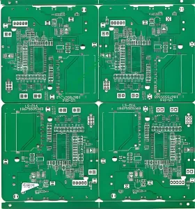
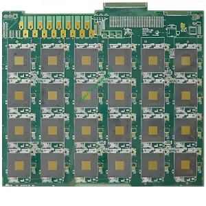
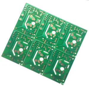
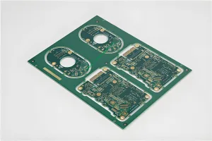
Introduction to Gold Finger Blind Hole PCB
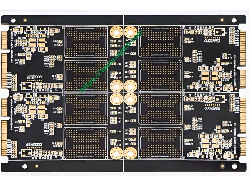
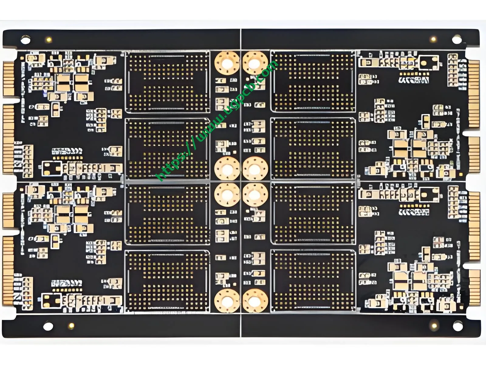
The Gold Finger Blind Hole PCB is a specialized type of printed circuit board (プリント基板) that features gold-plated fingers and blind holes. This design allows for enhanced connectivity and compact integration within electronic devices.
製品の概要
The Gold Finger Blind Hole PCB is constructed using high-quality S1140 FR4 material, ensuring durability and excellent electrical performance. It consists of four layers, with a copper thickness of 1OZ and a finished thickness of 1.2mm. The surface treatment involves immersion gold, which provides excellent conductivity and corrosion resistance.
アプリケーション
This type of PCB is primarily used in computer components, where high-speed data transmission and reliable connections are crucial. The gold fingers allow for easy plugging and unplugging, while the blind holes facilitate internal connections without the need for through-hole components.
分類
The Gold Finger Blind Hole PCB can be classified based on its layer count, 銅の厚さ, and special processes such as blind and buried vias, as well as the presence of gold fingers and blind holes.
材料
The base material for this PCB is S1140 FR4, a flame-retardant glass-epoxy laminate that offers excellent thermal stability and mechanical strength.
パフォーマンス
With trace/space dimensions of 4mil/4mil (0.1MM/0.1MM) 0.2mmの最小穴サイズ (8ミル), the Gold Finger Blind Hole PCB is designed for high-density interconnect applications. The immersion gold finish ensures low contact resistance and long-term reliability.
構造
The PCB consists of four layers, with blind and buried vias allowing for complex routing between layers without the need for through-hole components. The gold fingers provide an edge connector interface for easy integration into larger systems.
特徴
Some key features of the Gold Finger Blind Hole PCB include:
- High-density interconnect capability
- Low contact resistance due to immersion gold finish
- Durable and reliable construction with S1140 FR4 material
- Compact design with gold fingers and blind holes
製造工程
The production process for the Gold Finger Blind Hole PCB involves several steps, 含む:
- 材料の準備: Selecting the appropriate S1140 FR4 material and cutting it to size.
- レイヤースタッキング: Stacking the layers of the PCB with precise alignment.
- Copper Etching: Using chemical etching to create the desired circuit patterns on each layer.
- Via Drilling: Drilling blind and buried vias to create internal connections between layers.
- メッキ: Applying copper plating to the vias and other exposed copper areas.
- 表面処理: Applying immersion gold to the surface of the PCB for improved conductivity and corrosion resistance.
- Assembly: Assembling the gold fingers onto the edge of the PCB for easy connectivity.
Use Cases
The Gold Finger Blind Hole PCB is ideal for use in computer components where space is limited and high-speed data transmission is required. Examples include motherboards, グラフィックカード, and other high-performance computing devices.
 UGPCBのロゴ

